


Lidar Sensors

(Courtesy of Fraunhofer Institute)
Better, smaller and further
Lidar sensor developers continue to improve the performance of their products and enable a wider range of applications, writes Nick Flaherty
Lidar sensors are a key element in the design of many uncrewed platforms. A near-infrared laser, invisible to surrounding people, can provide detection of obstacles at distances of up to 300 m for driverless cars and trucks, or at ranges of 10-50 m for industrial robots. Sensor developers have used a number of techniques to boost the range and reduce the size and cost of such devices, with many designs moving to micro-machined and solid state approaches.
New techniques for assembling the sensors are also being explored to reduce costs, by combining the lasers, mirrors and sensors under a glass dome to provide the optics in a fully automated assembly process. This can help to reduce the size and cost of the sensors, and improve performance.
New approaches to the design of Lidar sensors are also driving down the size and cost with more integration. Metamaterials built from nanoscale structures are opening up new ways to reduce the size and weight of the sensor units to enable more applications, including airborne designs.
A Lidar sensor has four main function blocks: transmitter, receiver, modulator and controller. The transmitter block includes the laser module, transmitter optics and a scanning system. This can be a micro-machined mirror, a diffraction grating or metamaterial modulator to steer the beam. Sensor makers tend to combine technology from different suppliers with a key element to provide a performance advantage.
The receiver block consists of receiver optics, a receiver array such as an image sensor from a camera, and receiver processing chips, which process multiple channels of the read-outs.
Techniques for flash Lidar avoid the need for a modulator by using an array of lasers based on a vertical cavity surface emitting laser (VCSEL) and a receiver, and using complex digital signal processing to process the returning data into a point cloud.

The controller can be implemented in a microcontroller or a custom ASIC, and the programming interface for this controller is becoming a key factor in the design of the sensor. Having an open API to the controller allows system developers to implement the higher-level system code more easily.
This extends to pre-processing algorithms that can allow developers to swap easily between different types of Lidar for different parts of an uncrewed platform, for example by using a long-range sensor for the front and shorter-range devices around the bottom of a vehicle.
Time-of-flight
One of the early techniques for Lidar was time-of-flight (ToF), where the time taken for the laser signal to bounce off an object determined the distance. However, this has significant drawbacks that make it difficult to use in many 3D vision applications. It requires detection of very weak reflected light signals, so other Lidar systems or even ambient sunlight can easily overwhelm the detector. It also has limited depth resolution and can take a long time to densely scan a large area such as a highway or factory floor.
To tackle these challenges, researchers are turning to a form of Lidar called frequency-modulated continuous wave (FMCW), which is based on ToF principles.
They have used techniques from medical imaging to improve the data throughput of FMCW Lidar by 25 times while still achieving sub-millimetre depth accuracy. Optical Coherence Tomography (OCT) is the optical analogue of medical ultrasound, which works by sending sound waves into objects and measuring how long the signals take to come back, similar to ToF. To time the light waves’ return times, OCT devices measure how much the phase has shifted compared to identical light waves that have travelled the same distance but have not interacted with another object.
(Courtesy of Sony Semiconductor)
FMCW Lidar uses a similar technique. When the detector gathers light to measure its reflection time, it can distinguish between the specific frequency pattern and any other light source, allowing it to work in all kinds of lighting conditions at very high speed. It then measures any phase shift against unimpeded beams.
A diffraction grating breaks the laser into a range of frequencies and allows the system to quickly cover a wide area without losing much depth or location accuracy. A technique called time frequency multiplexed 3D coherent ranging looks only for the peak signal generated from the surfaces of objects. This costs the system a bit of resolution, but with much greater imaging range and speed than traditional Lidar.
This technique generates 475 depth measurements along the axis of the grating axis within a single laser sweep, generating an overall acquisition rate of 7.6 MHz. This approach enables real-time 3D imaging results of various everyday objects including a living human hand with a maximum imaging range of 32.8 cm and a 3D frame rate as high as 33.2 Hz.
(Courtesy of TU Wien)
The Lidar controller can be implemented in an FPGA and a microcontroller. The system in the FPGA includes the control of the laser pulse timing according to the mirror movements, ToF calculation based on the receiver signal, and functional safety to ensure safe operation of the Lidar, especially eye safety.
The microcontroller has multiple cores inside, which are used for defining the starting sequence of the Lidar as well as the packet generation of the point cloud measurements for data transfer to an external PC via Ethernet.
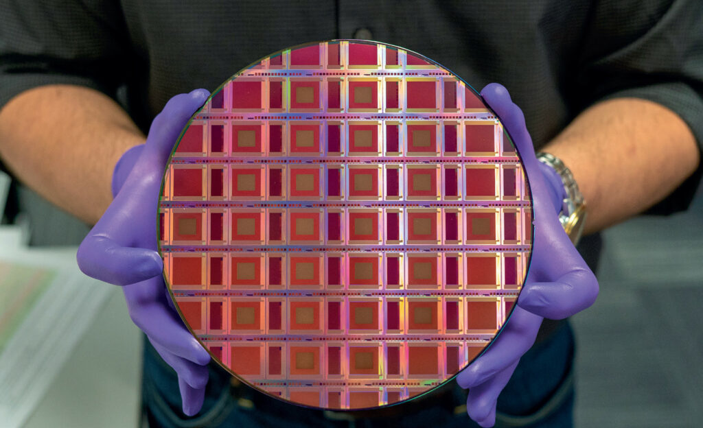
SPAD ToF sensor
A stacked sensor using a direct ToF (dToF) method is an industry first for automotive Lidar applications. This uses 10 μm2 single-photon avalanche diode (SPAD) pixels and distance measuring processing circuit on a single chip, resulting in a 1/2.9-type form factor with a 6.25 mm diagonal.
The SPAD pixel structure uses avalanche multiplication to amplify electrons from a single incident photon, causing a cascade.
(Courtesy of Fraunhofer Institute)
SPAD pixels are used as a type of detector in a dToF sensor, which measures the distance to an object by detecting the ToF (time difference) of light emitted from a source until it returns to the sensor after being reflected by the object.
The sensor uses the same stacking and copper-to-copper connections as those for CMOS image sensors to combine a chip with 100,000 SPAD pixels in a 597 x 168 array, with the distance measuring processing circuit on a second chip. The copper pads are included in the pixel array to provide the connection to the processing chip.
The sensor also uses a light incidence plane with irregularities on its surface to refract incident light, thereby enhancing the absorption rate.
These features result in a 24% photon detection efficiency in the 905 nm wavelength commonly used by automotive Lidar light sources. That makes it possible to detect distant objects with a low reflection rate at high resolution and distance resolution.
An active recharge circuit is included on the circuit section, which comes with a connection for each pixel. This allows a response speed of 6 ns at normal operation for each photon.
This stacked construction enables a Lidar sensor with a range of 300 m and an accuracy of 15 cm using a 6 x 6 block of pixels, or a resolution of 30 m with a 3 x 3 pixel block. A mechanical scanning Lidar reference design with a rotating polygon mirror has been developed using a 905 nm laser and the SPAD sensor for evaluating the sensor.
3D imaging
Researchers have also found a way to use standard image sensors to provide 3D Lidar images with a new type of low cost modulator.
Using a technique called acoustic resonance, researchers have built a simple acoustic modulator using a thin wafer of lithium niobate, a piezoelectric material, coated with two transparent electrodes.
When electricity is introduced through the electrodes, the crystal lattice of the lithium niobate vibrates at very high, very predictable and very controllable frequencies, rotating the polarity of the light. This can be used to modulate the light, and the geometry of the wafers and the electrodes defines the frequency of light modulation to fine-tune the frequency.
A polarising filter is placed after the modulator that converts this rotation into intensity modulation, providing modulation at 3.7 MHz across a 1 cm2 area.
The modulator design is simple, and integrates into a proposed system that uses off-the-shelf cameras to build an integrated Lidar for UAVs and space rovers where power consumption is key. The researchers have cited a voltage of 2 V peak to peak to drive the modulator, and say they have further reduced the energy consumption by at least 10 times, with a reduction of 100 times being possible.
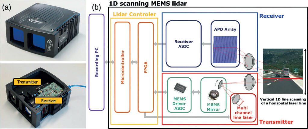
MEMS mirror
Rather than using a rotating mirror, a micro-machined MEMS mirror is becoming increasingly popular for modulating the laser beam in the sensor. However, these can struggle with ageing as the switching at megahertz speeds puts a strain on the nanoscale metal used to move the tiny mirrors. The design of the MEMS mirror array also has a key impact on the field of view.

Vibration is a key issue as well for sensors using MEMS mirrors. Even tiny vibrations can have an impact on the accuracy of the laser beam at the 200-300 m distances required for driverless cars. Researchers have evaluated a prototype of a long-range, 1D prototype sensor that can detect a tyre on the road from 130 m.
Compared with the other scanning methods, 1D scan Lidar is a hybrid of the flash Lidar and 2D point-scanning Lidar, allowing a high frame rate with fewer laser pulses and less complexity in sensor read-out. However, generating a uniform laser line is not trivial with commercially available laser arrays. High laser power is still required owing to the broadening of the laser into a line along one axis.
That limits the detection range since the light sources must comply with Class 1 laser specifications. The MEMS scanning system also has to be highly robust against harsh environmental conditions such as vibrations, shocks and temperature variations.
To achieve this stability, an ASIC senses the timing of the MEMS mirror movements with nanosecond accuracy, and secures a stable oscillation by using a digital controller.
Experimental results reveal that the MEMS control in the ASIC can successfully suppress the errors caused by vibrations. For the MEMS Lidar without the controller, the applied random vibration distorts the 3D measurements along the scan axis, leading to errors in the 3D surfaces and small, flying particle-like points around the edges of the objects.
When the control of the MEMS mirror is turned on, these errors are reduced significantly, allowing reliable 3D object detection and ranging. The MEMS controller reduces the influences of innate vibrations with automotive Lidars and maintains stable 3D images, enabling reliable image processing and object detection. This is the key technique for operation under vibrations and shock.
The 1D scanning MEMS Lidar exploits a multi-channel horizontal line laser to scan the scene vertically for a 10 x 11º horizontal and vertical field of view at a frame rate of up to 29 Hz. This was tested to the LV124 automotive standard, where the vibration tests are performed in three conditions – open loop without control and two phase-locked loops (PLLs) – with default and high-gain settings.
The test results demonstrate that vibration can cause wobbly distortion along the scan angle in the open-loop case, and the PLLs can effectively suppress this influence in the mean and standard deviation of the standard point to a surface error of up to 69.3% and 90.0% respectively. This verifies the benefits of the MEMS mirror control, ensuring stable point cloud measurements under vibrations in harsh automotive environments.
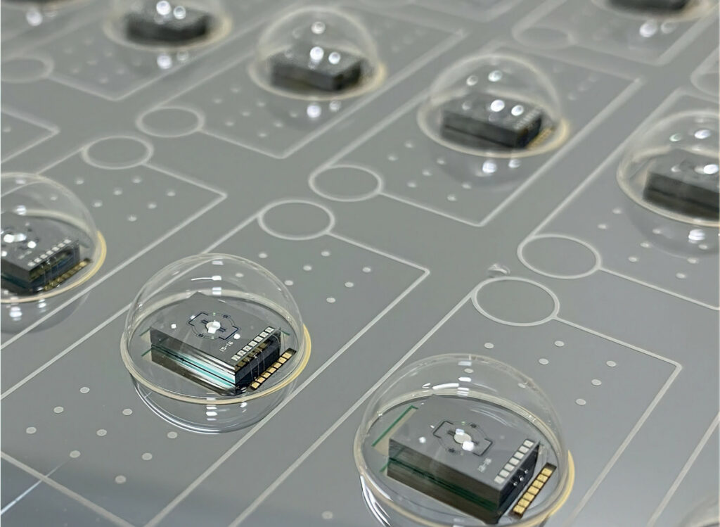
Encapsulating MEMS mirrors
One way to make the MEMS mirrors more robust against environmental issues, including vibration, is to encapsulate them in glass domes that also act as the optics.
The shaping of various types of glass has proven to be particularly significant. After all, with the integration of optical functions into the world of microsystems, packaging components and systems at the wafer level is a key challenge.
The process allows the fabrication of precise optical components at the wafer level for different applications at low cost. As borosilicate glass for the optics has a similar coefficient of thermal expansion to silicon, it is suitable for anodic bonding, which involves heating and applying an electric field to the substrate materials. Anodic bonding is also called field assisted bonding or electrostatic sealing.
This produces a material compound that remains stable even under large temperature changes.
If the silicon wafer includes structured recesses, the glass can be moulded into these embossed recessed structures when the silicon-glass bond is raised to temperatures above the transformation temperature of the glass. The glass then becomes a highly viscous fluid that can be pressed into moulds, for example, when the external pressure exceeds the gas pressure in the recessed moulds. The resulting glass structures are exposed by dissolving the original silicon wafer in a caustic bath.
This process of high-viscosity moulding has been further developed by using a low gas pressure in suitable furnaces to form shapes in a glass wafer by blowing. This allows glass shapes to be formed with the shapes determined only by the viscosity, surface tension and pressure conditions inside and outside the previously created volumes in the silicon wafer.
The surfaces of glass shapes generated in this way are created without material contact, and are therefore flat, with a roughness of less than 1 nm, which is essential for optical applications. As these shapes are produced on silicon wafers, a large number of optically identical components are always produced simultaneously, leading to low production costs.
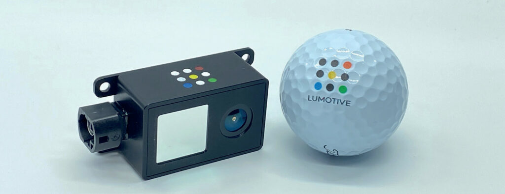
(Courtesy of Lumotive)
Alongside the glass manufacturing processes, simulation programs are also used to optimise the shaping. Optical measurement techniques have been set up to characterise the finished components.
The technology also makes it possible to feed electrical contacts through a glass wafer, or to precisely mount individual components such as laser diodes or lens elements on a carrier wafer using high precision laser soldering, and then to encapsulate them together with a suitable glass wafer. Virtually any desired optical or opto-mechanical assembly can be implemented, operated under vacuum or even filled with different gases.
MEMS switches
The same technique for building the mirrors is also being used to improve the performance of a modulator. Rather than use a mirror, MEMS structures are built on a standard CMOS chip-making process to use an electric field to switch the different beams from a laser array. This allows an array of 16,384 pixels on a 1 cm2 chip.
When the switch turns on a pixel, it emits a laser beam and captures the reflected light. Each pixel is equivalent to 0.6º of the array’s 70º field of view. A 3D image is built up by cycling rapidly through the array. A prototype system built using this design currently has a range of 10 m, although 100 m is definitely possible and researchers believe they can achieve a range of 300 m.
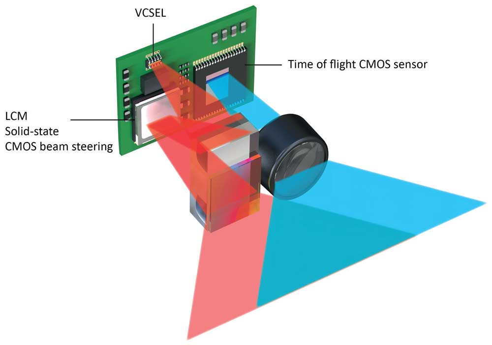
Metamaterial beam scanning
Another approach blends the worlds of ToF with digital cameras. The missing link for this is the beam steering. This uses a combination of a metamaterial built using semiconductor technology with a liquid crystal.
The metamaterial is created from 3D structures on the surface of a semiconductor chip that allows the phase of the incident light to be tuned. Each pixel on the surface is a phase delay element, and by programming many thousands of these elements with the right voltages the beam can be directed by combining constructive and destructive interference.
The infrared laser used in a Lidar has a small wavelength, typically 905, 940 or 1550 nm, so the structures need to be less than 100 nm. This is suitable for semiconductor manufacturing processes that can currently manufacture structures with a minimum feature size of 5 nm.
Adding the 3D optical structures allows the liquid crystal to switch in a smaller area and, critically, allows it to switch at speeds of microseconds rather than milliseconds. They are controlled by typical liquid crystal voltages with commercial off-the-shelf LCD drivers.
This also defines the pixel size, which allows a field of view up to 170º.
The size of the array, typically 1 sq in, aligns with the optical aperture and lens of the Lidar to determine the amount of light energy that emerges from the sensor. The fact that the metamaterial is reflective rather than transmissive allows all the laser light to be channelled out of the aperture. The higher the energy, the longer the range, and this approach can support a range of up to 300 m.
A reference design for a Lidar sensor with a VCSEL and ToF image sensor uses the metamaterial beam steering to provide a field of view of 120 x 90º with a range of 10 m in a sensor measuring 1 cm3 for applications such as UGVs and mobile robotics for close-range sensing. The target for this Lidar sensor in volume production is $10, allowing multiple sensors around an uncrewed system.
However, the field of view is software programmable, allowing a range of more than 200 m with a 20-30º field of view, or a 50-100 m range for one of 120º in a larger unit to allow for larger optics. The software-defined capability allows the Lidar to scan only to the angles of interest more frequently – the beam can hop around and focus where necessary.
The processing is via an API to define the angle and frame rate, and a scan controller takes care of all the details.
The 905, 940 and 1550 nm lasers need slightly different structures in the metamaterial to tune the laser signal, as well as for different types of sensors.
Combining Lidar sensors
One growing trend is to combine different Lidar sensors in one system. This can be to provide different levels of performance, for example with sensors optimised for long range and narrow field of view combined with those for a wide field of view. It can also be used to avoid problems in the supply chain, as being able to swap easily between different Lidar sensors in the same system can avoid production problems if some are in short supply.
The Lidar sensors can be combined with a pre-processing engine that connects to the output of the sensor to analyse the point cloud output. The engine provides a standard data format for the central processor to allow multiple sensors to work together, or to reduce the bandwidth of the data feed.
The bandwidth for a wireless network link from a UAV can be reduced by a factor of 50 just by sending the relevant data rather than the entire point cloud. All the data is stored on the Lidar sensors in the UAV’s payload, but providing realtime data allows an operator to assess the quality of the data capture as it comes in and adjust the flight path of the UAV if necessary.
These decisions could also be made autonomously by the UAV’s central processor.
Determining the relevant data and ensuring a common data format requires sophisticated algorithms. These have been run on ARM processor cores in a dedicated hardware unit, but are now being integrated into other hardware. This requires software virtualisation technology to provide real-time processing on ARM, x86 and RISC-V processors.
Combining mobile and static Lidar
The pre-processing capability and common data format also allows data to be combined with static Lidar sensors.
This approach is considered too complex to be able to use a synchronisation clock for all the data from multiple Lidar sensors, so instead the physical space is used to coordinate the data. This takes the feeds from each sensor and identifies areas that overlap, along with position data, allowing a broad point cloud to be constructed.
Conclusion
Lidar sensors continue to balance the demands of range, size and power consumption. Designs are reducing the power consumption of the modulator and increasing its reliability, whether through vibration control or the use of metamaterials, and are achieving ranges of up to 300 m for driverless cars. New techniques from the medical world are also improving sensor performance, while new manufacturing techniques are helping to boost their reliability and reduce costs.
With the wider range of different Lidar technologies being developed for uncrewed systems, so pre-processing algorithms can combine the data from different sensors, providing system designers with the ability to use the best sensor for a particular application.
Acknowledgements
The author would like to thank Raul Bravo at Outsight, Gleb Akselrod at Lumotive and Han Woong Yoo at TU Wien for their help with researching this article.
UPCOMING EVENTS


