


Embedded computing tech

Board behaviour
Designers are taking new approaches to embedded systems to pack in more power in ever-smaller forms, as Nick Flaherty reports
The drive to reduce size, weight and power (SWaP) in autonomous systems is an engineering challenge when faced with greater demand for more complex sensors and the resulting increase in embedded computing requirements. The task of balancing the latter with system and cost specifications covers embedded boards and the selection of the right level of processing power and consumption.
The drive to add machine learning to process sensor data is also pushing up compute requirements with computer-vision algorithms based on transformer neural networks.
Transformers are a more complex AI framework, requiring higher processing power, and they are being used in centralised control devices for driverless trucks. But this technology is also being adopted in driverless cars, tapping into speech-to-text capabilities as the user interface for passengers.
The latest generation of graphics processing units (GPU) are being used as accelerators for these algorithms in the monolithic system-on-a-chip designs that are coming in 2025.
New approaches such as chiplets are enabling smaller compute systems with higher performance, providing a mix of capabilities, including different AI accelerators. Such devices for centralised controllers in driverless cars are now emerging as samples, with production scheduled for 2026.
But all of these approaches need to address the key issues of reliability and long-term supply. Boards need soldered-down processors and memory to tackle the reliability issues caused by vibration, and the more complex chiplet devices need to be qualified to automotive and aerospace quality standards, such as AECQ-100 and AECQ-200, respectively.
Long-term supply often means decades of availability. This can be a key restraint on the adoption of suitable embedded computing technologies for uncrewed systems.
Board formats
The latest emerging board format for embedded computing in uncrewed systems is VNX+ or VITA90. This is built on VME standards that have boards connected to a backplane to flexibly build up a system. The cards can be sensors, processors or switches, along with a power-supply card.
VNX+ is an enhancement of the VITA 74 specification for small form-factor boards that can fit into the fuselage of a UAS. The main changes are to increase the thermal envelope from 20 W to 80 W for each card, allowing more powerful processors and GPUs to be used, and also to increase the signal speed across the backplane to 110 GHz to support higher data-rate protocols, such as gigabit Ethernet.
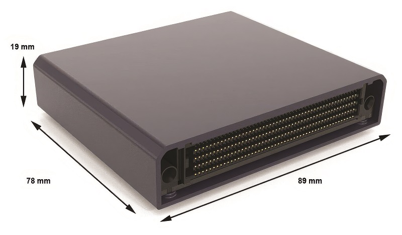
The VNX standard form factor is 89 mm x 78 mm, with height options of 12 mm or 19 mm – about one-third of the volume of a traditional, 3U plug-in card. The specialist connectors have a 1.27 mm pitch for the smaller size, and they are designed to be high-speed and high-density with an open-pin field design.
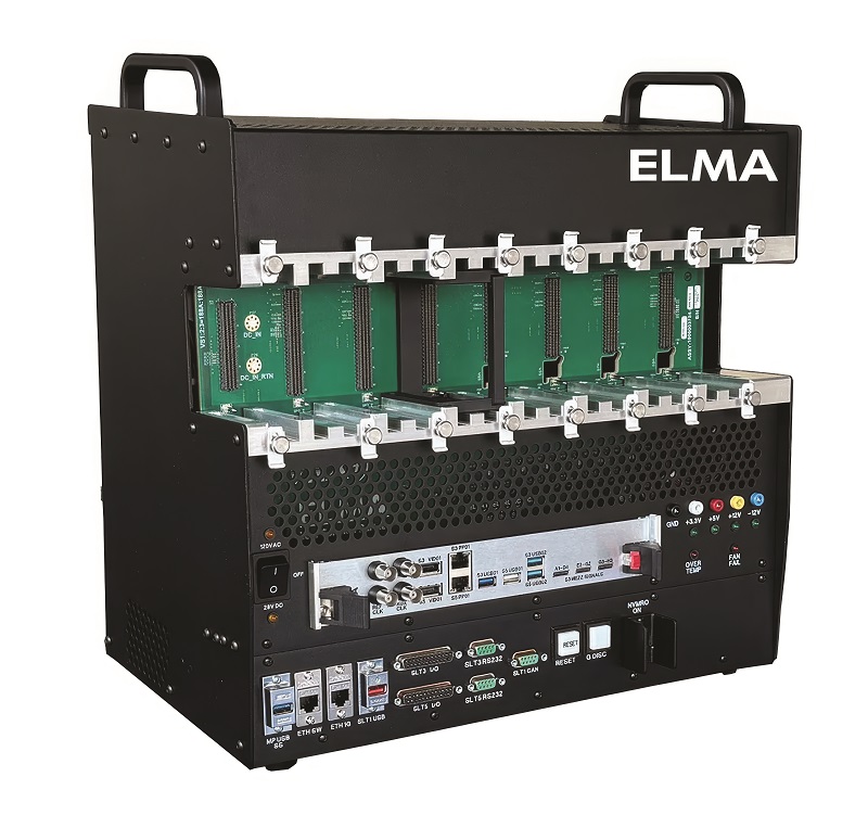
Development chassis are providing the ability to combine different VNX+ boards to test the overall system performance. The VNX+ specification ensures the boards are compliant with the modular open systems architecture (MOSA) that allows interoperability with a wide range of software and sensors.
The eight-slot backplane in the development chassis supports up to 10GBASE-KX/40GBASE-KX4 Ethernet and PCI Express 4.0 with six well-defined payload slots that can accommodate a range of cards, one switch slot and a PSU slot. An internal power supply, gigabit Ethernet switch, a VITA 46.11 chassis manager, maintenance port aggregator and front-panel I/O are also integrated into the chassis.
The chassis supports the 19 mm x 320 pin, 19 mm x 400 pin, 39 mm x 320 pin and 39 x 400 pin plug-in cards, while the 320 pin variants support the hybrid aperture connectors with custom connector pinouts that fit into the existing chassis slot, or aperture.
The unit has handles for easy transport in the lab and field, a 5o tilted card cage and locking retainers to secure modules in slots against blind-mate connector-spring forces. It uses directed air to cool modules, either with or without metal enclosures, and offers built-in I/O, including unique external I/O (UEIO) direct device control without additional mezzanine cards.
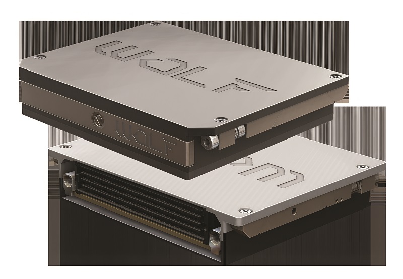
A small number of VNX+ boards are available commercially, but the flexibility of the standard lets engineers design and build their own specialist sensor or security boards while using commercial compute, switching and power boards to simplify the development process.
These include VNX+ boards using a GPU with 1024 cores running up to 918 MHz, providing general-purpose processing. The chip includes 32 third-generation Tensor cores for AI machine learning, achieving a performance of up to 100 TOPS (with 8 bit integer data).
Despite the small form factor, the board includes a self-encrypting drive that supports data encryption, providing protection for sensitive information without significantly affecting read/write speeds to the drive.
PC/104
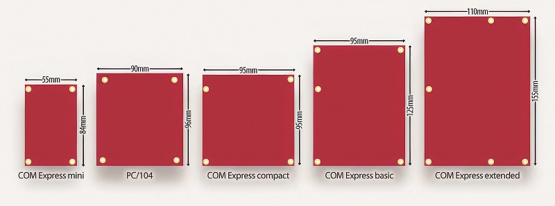
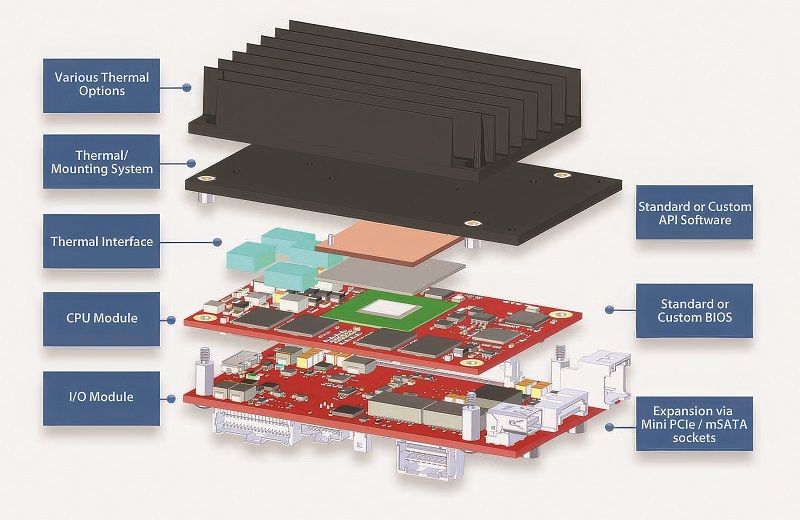
There are also other long-term, small form-factor board formats; notably, the 90 x 96 mm PC/104 that can be built into a stack with sensor and processor boards. This has been used for many years since being standardised in 1992, and while it may have been superseded in many areas by the COM Express specification, it still has key advantages; the primary one being that the PC/104 boards are more rugged and do not use a separate processor module that can have reliability issues.
PC/104 embedded processing units (EPU) can be built from a CPU board, I/O board and integrated heat plate. The resulting unit has a footprint about half the size of equivalent single-board designs and is mechanically rugged with standard mounting-hole locations.
The EPU concept simplifies the making of modifications to meet specific I/O needs. Existing products can be configured by modifying the I/O portion of the product, or, if greater modifications are required, a fully custom I/O board can be created for an existing board set. With the two-board concept, these modifications come at a lower cost and shorter lead time than other solutions.
This approach also provides a processor upgrade path. Often, a newer CPU board can be paired with an existing I/O board to significantly upgrade a system, providing upgraded performance, memory capacity or extended product life without any I/O or cabling changes.
For example, a new-generation CPU card can be added to an existing I/O card to boost the performance.
For example, one company’s Owl EPU is a combination of a previous EPU I/O board and a new-generation CPU.
Environmental testing means that EPUs are fully verified to operate in extreme environments, including the full industrial operating temperature range of -40 to 85 C and MIL-STD 202 conditions of shock and vibration. The mounting points, connectors and small cross-section of the PCBs limit board flex, and also provide excellent performance in high shock and vibration environments.
One of the drawbacks, as with VNX, has been the lower performance of older standards. However, PC/104 has been updated with the faster PCI Express connectivity standard to support the latest processors and interfaces. This allows an EPU to use the mini PCIe or M.2 socket to add expansion modules or boards with almost no size penalty. Examples include additional Ethernet, video, GPIO and other I/O ports, as well as solid-state storage devices.
PC/104 boards are using the latest Intel Xeon E 6 processors, the refresh of the Coffee Lake family with up to 32 GB of error-correcting memory, fast onboard NVMe SSD storage and TPM 2.0 security. The error-correcting memory makes it indispensable for mission-critical applications and aeronautics applications at higher altitudes.
The board is aimed at intensive processing, particularly applications with security concerns or where limited communication bandwidth precludes sending raw data back to a data centre.
Several built-in interfaces include 1 Gbit and 2.5 Gbit Ethernet, USB 3.1, serial ports, I2C, GPIO, analogue input/output (ADC/DAC) and Mini DisplayPort output. Onboard expansion includes one Mini PCIe slot and two M.2 slots, which can support functions such as 5G cellular, AI accelerators, GPS, flash data storage, analog and digital IO, additional data storage (SSD), display interfaces, wi-fi, Bluetooth and Ethernet.
Modifications for the EPU include conformal coating, revision locks, custom labelling, customised testing and screening. For driverless cars, there is a significant move towards centralised computing power. This is mostly based on a GPU processor and software stack.
The system-on-a-chip combines GPU cores with 167 TOPS of performance with custom deep-learning accelerators for 87 TOPS and 12 ARM Cortex A78AE automotive-qualified processor cores. An image signal-processing block can handle 1.85 Gigapixels/s from 12 cameras over a 90 Gbit/s link, with a 30 Gbit/s link for Lidar.
Nine CAN interfaces provide connectivity to the rest of the system, which has a high-speed interface to low-power LPDDR5 memory, which is 256 bit wide. Two of these are used for the central controllers in self-driving vehicle prototypes from Volvo, Li Auto, Great Wall Motor (GWM), Zeekr and Xiaomi.
The next-generation system-on-a-chip adds the latest GPU architecture and ARM Cortex-A720AE cores, also qualified for automotive reliability, to provide twice the performance at 2000 TOPS.
Chiplets for performance
A relatively new technology called chiplets (as indicated) is being used for the centralised controllers in a vehicle, requiring a different architecture.
These typically have a central system-on-a-chip device that handles most of the central processing, which is mounted on a substrate and connects to different chips, whether these are memory, including the latest high-bandwidth memory (HBM3e) or an AI accelerator, called a chiplet. These chiplets do not have a direct connection to the rest of the system, but go through the central controller chip.
There are also various types of substrate. These on-die interconnect technologies include organic substrates similar to a printed circuit board, embedded silicon bridges (EMIB), silicon interposers and fan-out embedded bridges. All have different speeds for the connection between the central chip and the chiplet, as well as varying interconnect densities to fit more chiplets onto the substrate.
But this does provide the ability to build a more complex, larger system on substrate without being limited by the maximum size of a monolithic chip.
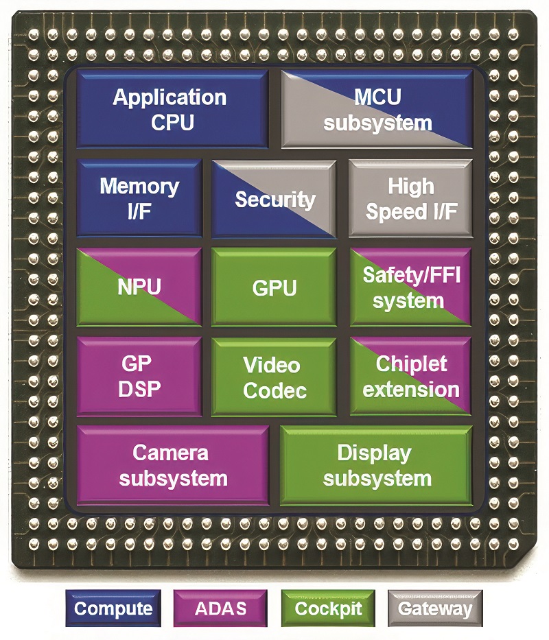
One of the first devices to use chiplets for automated driving has a complex combination of 38 ARM cores in a system-on-a-chip that links to AI and GPU chiplets in a single package connected by the Universal Chiplet Interconnect Express (UCIe) (discussed below). This combination allows the chip to run multiple automotive domains, including advanced driver assistance systems (ADAS), in-vehicle infotainment (IVI) and gateway applications.
This supports the key shift to centralised electronic control units (ECUs), which is key for driverless cars. The automotive-qualified N3AE 3 nm semiconductor-manufacturing process provides higher integration, alongside a 30-35% reduction in power consumption compared with devices designed in the previous 5 Nm process node.
This increase in power efficiency can lower overall system costs by eliminating the need for additional cooling with the higher embedded compute capability.
The key to the implementation of multiple domains is a proprietary, hardware-based isolation technology for the 32 ARM Cortex-A720AE CPU cores with 1,000 K DMIPS, alongside six Cortex-R52 real-time cores delivering over 60 K DMIPS. These R52 cores have a dual lockstep capability that allows one controller to check the operation of safety-critical software processes on a step-by-step basis, only continuing if both agree on the result.
This is a key way to achieve the highest safety level of ASIL D in the ISO 26262 standard without needing external microcontrollers to perform the checks.
The hardware isolation technology isolates safety-critical functions such as brake-by-wire from non-critical functions. Those deemed safety critical can be assigned their own separate, redundant domains, each with their own independent CPU core, memory and interfaces, preventing potentially catastrophic vehicle failure in the event of a hardware or software fault from a different domain.
A neural processing unit provides up to 400 TOPS of AI performance and a GPU provides processing up to 4 TFLOPS, both built into the chip. But other accelerators can be added to the system-on-a-chip using the UCIe interface, which can scale the AI processing by three to four times to exceed 1000 TOPS.
Die-to-die standards
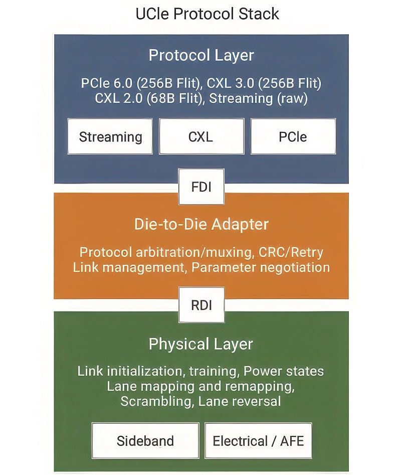
The UCIe standard was introduced in March 2022 to help standardise die-to-die (D2D) connectivity in multi-die systems. It can streamline interoperability between dies on different process technologies from various suppliers.
UCIe works by defining a set of protocols and physical layer specifications that govern communications between chiplets, as well as the software model, and can work with any substrate technology. This standard ensures data can be transmitted at high speeds with minimal latency and power consumption. It also has added-in redundancy that can help with the manufacturability of devices and the overall reliability of an end device.
The physical layer (PHY) deals with the electrical characteristics and signalling methods used in data transmission. UCIe specifies a high-speed, low-power physical layer that supports data rates of up to 32 Gbps per pin as per the v2.0 specification.
The D2D adapter layer takes care of link management functionality, as well as protocol arbitration and negotiation. It includes the optional error-correction functionality, which is based on a CRC and retry mechanism.
The protocol layer defines the rules and conventions for data exchange, including command sets and response formats, ensuring compatibility between chiplets from different manufacturers.
The specification offers redundant lanes between the two sides of the physical interface, or PHY, enabling repairs through the extra lanes. Whether connected to the outside world or not, all die must be accessed, tested and repaired through the UCIe channel, which also enables monitoring of ongoing die issues.
UCIe for automotive
UCIe is increasingly seen as an open interconnect to mix and match various chiplets. To better evaluate automotive requirements, it made a number of enhancements.
For preventive monitoring, the UCIe 1.1 specification adds new registers to capture eye margin (eye width and height, if applicable) information in a standard reporting format while a link is optimised; also called training. System software can trigger periodic retraining of the link to gain eye margin information using the existing UCIe 1.0 mechanism.

The specification also defines how to inject test bits into the links at run time to check the mechanisms of UCIe 1.0 are working correctly. Any errors detected during the process will be reported in the UCIe 1.1 per-lane error-log register with the ability to send interrupts. System software can then use this information to assess whether link repair is needed.
UCIe 1.0 supports streaming interconnects such as the AXI, CHI and symmetric multiprocessor (SMP) coherency protocols that connect up the blocks in a chip and run over the UCIe link to the chiplets. UCIe 1.1 keeps this raw mode, but the streaming protocols can now use the D2D adapter interface, so they reuse the redundancy checking, retry and power-management features in existing blocks in the system-on-a-chip or a chiplet.
UCIe 1.1 can also work with other protocols with on-demand interleaving. This enables the coexistence of multiple protocols (like streaming for processing, PCIe for discovery, DMA, TLB, error reporting, interrupt, etc) for new uses.
UCIe 2.0
The UCIe 2.0 Specification adds support for a standardised, system-management architecture that can be used in all the different chiplets to control and debug a device.

The manageability features are optional and work with the UCIe Debug Architecture (UDA), which includes a management fabric within each chiplet for testing, telemetry and debug functions, enabling chiplets from different suppliers to work together.
The 2.0 Specification also supports 3D packaging. Rather than having the chips, memory and chiplets laid out flat,
UCIe-3D is optimised for hybrid bonding in a stack, much like the PC/104e boards. The bump pitches for this vary from as big as 10-25 microns to as small as 1 micron or less to provide flexibility and scalability.
Tooling up
Using chiplets means designing the system in various ways and the same package may hold different chiplets, providing varying levels of embedded performance. New automated tools are enabling engineers to explore the best options for vehicle design as the options are so wide now.
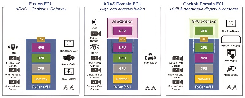
For the next generation of electrical and electronic controllers, systems are grouped by physical location with central compute in a zonal architecture, but there are scalability challenges. There is a gap in compute performance between the low end at 100 TOPS and the high end of 1000 TOPS, and from 100 Gb/s to 1000 Gb/s in memory bandwidth.

A low-end design starts with a chiplet for the interfaces, or the IO chiplet. This is a monolithic die that can also handle minimal processing for low-end applications as a fusion chip that controls cameras and displays. For more performance there is a computing extension.
Automated driving systems can add an ADAS chiplet to handle more cameras and sensors. This leads on to nine system options that need new tools to explore the design space.
Instead of designing nine separate chips, the tool can define three chiplets for five architectures for each segment with four packaging options: two for standalone, low-cost platforms, I/O + Compute; and four of the ADAS chiplets.
These variants have been tested in a simulator called VPSim as virtual prototypes for benchmarking, which has a good trade-off between speed and accuracy, but this is not good enough for the chiplets.
The design flow includes automated exploration of the design space, so that from just the parameters, candidate devices can be identified and the key performance indicators (KPIs) extracted to generate the binaries for the virtual models to perform the benchmarks.

FPGAs
Processors and GPUs are not the only way of providing the embedded compute capability for uncrewed systems. While chiplets can provide some additional standard functions, sometimes that is not enough and custom logic is needed. Field-programmable gate arrays (FPGAs) combine an array of reconfigurable logic with a hardware processor subsystem and high-speed interfaces.
While previous generation FPGA devices have used chiplets to integrate interfaces built on a different process technology from the main array fabric, these interfaces are now being combined in monolithic devices to provide more performance in a smaller size.
The latest pure automotive FPGA slims down the packaging to 9 x 9 mm from the previous 19 x 19 mm, with 81,000 cells for configurable logic and 3.8 Mbits of memory. This comes from moving to a 16 nm process that enables a smaller die for sensor fusion and implementing custom signal-conditioning algorithms.
Conclusion
Several forces act on embedded computing systems for uncrewed systems. Reducing size, weight and power is key, but with higher performance for the same thermal profile to minimise any increase in cooling requirements.
A new generation of standards, such as VNX+, will help engineers design complex systems with a smaller form factor around a standard backplane for UAVs. These boards will host the GPUs and processors being used to provide automated driving. The next-generation Thor GPU will enable fully self-driving vehicles in a big shift for embedded computing systems.

Acknowledgements
With thanks to Mark Littlefield at Elma Electronics and Manuel Mota at Synopsys.
UPCOMING EVENTS


