


Data Storage
Autonomous vehicles need a safe and secure, centralised computing engine with sufficient memory storage, writes Nick Flaherty
Data, data everywhere
The demands of high-performance sensors, coupled with artificial intelligence (AI) and machine learning (ML), are driving up the requirements for data storage in uncrewed systems, both during the development phase and in operation.
For driverless cars and trucks in particular, the storage requirements are running into terabytes of data, taking streams of information from radar, Lidar and cameras, as well as large ML models. Whether this storage is used and then discarded, stored locally on the vehicle or sent to the cloud is a key architectural decision.
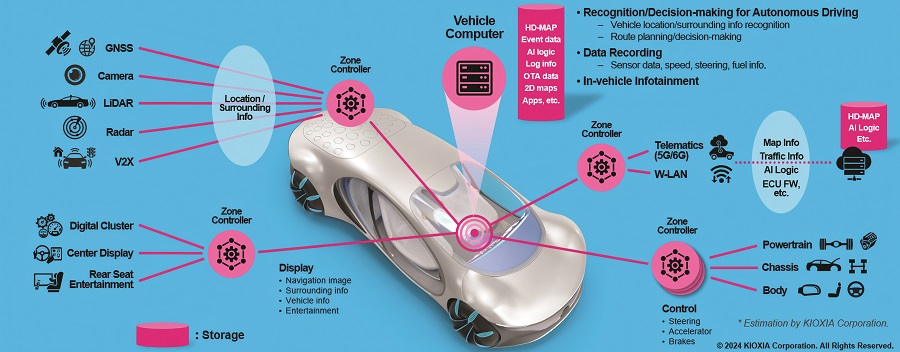
The architecture of the autonomous vehicle (AV) is moving towards a centralised computing engine with a software-defined architecture, requiring significantly more memory for the code that runs the vehicle. It must be secure, reliable and able to be updated over the air (OTA), which places key requirements on memory storage.
Various memory technologies and standards are being adopted. Multi-level NAND flash provides high-density storage for data from sensors and local AI frameworks, while NOR flash is used for millions of lines of code. With software footprints expected to expand from 100 million lines of code in today’s high-end vehicle to something in the order of one billion in future, automotive memory has become a key consideration.
The demands on memory and storage performance to achieve autonomous operation are driving the need for higher memory bus widths at 256 bits and 512 bits, which operate at an input/output (I/O) signalling rate of 8.5 Gbit/s.
This has to be achieved with functional safety to accommodate random and systematic fault coverage. This safety framework provides guidance when considering breakthrough automotive memory solutions and support.
There are significant advantages to improving data storage with centralised architectures in AVs. This can reduce the weight of the wiring and therefore the weight of the vehicle by 20 kg, leading to a potential increase in range of up to 4,000 miles per year.

Developmental challenges
The major challenge for data storage is during the development phase. AV algorithm development requires data from many vehicle sensors, including more than 12 cameras, infrared, Lidars, radars, ultrasonic sensors and other parameters, which create over 100 TB of data per car per day. This data is recorded and transferred in a variety of ways to remote data centres for algorithm development – from consumer-grade storage drives in large bays within the vehicle to integrated data-loggers and storage devices.
In both instances, security, scalability and transfer costs are exceedingly expensive and challenging. Solutions can cost more than $200,000 per vehicle to support the capacity required. For a fleet of 100 vehicles, that is more than $20m in upfront costs to secure the required data storage.
Additionally, these solutions require new capex purchases of storage components as technology continues to push boundaries towards fully automated vehicles. AV developers need a more cost-effective and scalable solution to gain access to more data faster.
The collected data needs to flow from vehicle to data centre, where the required computing platforms are housed. Unfortunately for the Tier 1s and car makers, this means becoming an IT expert in the Internet of Things (IoT) and the edge/macro edge.
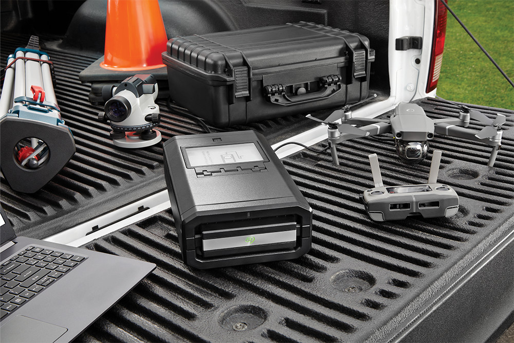
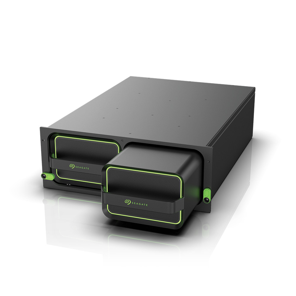
Using edge storage and data transfer as a service provides a cost-effective way of managing more than 100 TB, all engineered to withstand harsh, mobile environments and enabling in-vehicle data ingestion up to 7 Gbit/s. A portable, rackable system records AV data by securing it to the trunk of the car, and a PCIe adapter can be used for an external PCIe port on the recording system or with self-encrypting drives.
The mobile data-storage system is built with industry-standard, AES 256-bit hardware encryption and key management in a rugged, lockable transport case for superior data transport and security. It is also agnostic to data logger form factors and architectures. The current research and development for AD vehicle technology requires use cases for rapid prototyping, real-time vehicle testing, calibration and logging, and many more.
Each test vehicle is, in effect, a mobile data centre, generating around 100 TB a day of data from the multiple sensors inside it. This data must be fed into a data lake, from which it can be extracted, and used for AI and ML modelling and training. The end result is AI/ML model code that can be used in real life to assist drivers by taking on more driving responsibilities.
The problem is that there can be 10, 20 or more test vehicles, each needing to store logged data from multiple devices. Each device can store its own data (a distributed concept) or use a central storage system.
Each method costs money. Just putting in-vehicle data storage in place can cost up to $200,000 per vehicle. That means a 50-vehicle fleet needs capital expenditure of up to $10m just to store the data, let alone use it.
Centralising the data can be done in two ways: move the data across a network or move the data-storage drives. Once in the same data centre as the AI training systems, the data has to be made available at high speeds to keep the GPUs busy.
Networking the data is costly and, unless the automobile manufacturer spends a great deal of money, it is slow. A fleet of 20 vehicles could each arrive at the edge depot on a daily basis with 100 TB of data. That’s 2 petabytes (PB) of data to upload per day. It is cheaper and perhaps faster to just move the drives containing the data than to send the bytes across a network link.
There are five problem areas in this data pipeline: the in-vehicle storage; data movement from vehicle to data centre; data-centre storage; and feeding data fast to GPUs.
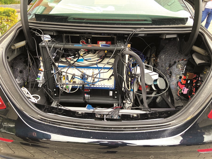
(Image courtesy of University of Limerick)
AI training
Each test vehicle has a disk drive array in its trunk, which takes data streamed from sensors to data loggers and stores it centrally. When a test car returns to its depot, the drives inside data cartridges can be removed and physically transported to a receiver unit in the AI/ML training data centre.
Once it arrives at the data centre, the data can be stored in an object storage system and also in the cloud for longer-term retention. Active file management (AFM) software feeds the data from the object storage system into a parallel file system and non-volatile flash storage. This is then accessible to the GPUs for model training.
In-vehicle data storage
Storing data during the life of the vehicle is another challenge. Code data tends to be stored in non-volatile NOR flash memory, which stores one bit per cell for reliability, and speed of writing and recalling the data. This enables instant-on performance and fast system responsiveness in automotive applications, but also limits the capacity of a memory device.
Current automotive NOR flash devices have a capacity of up to 2 Gbit, and data-transfer rates of up to 400 Mbit/s read throughput or 166 MHz single transfer rate, 166 MB/s read throughput using a 200 MHz clock double data rate (DDR) with data strobe.
The NOR structure enables 75.8 ns initial access time and 2.5 ns subsequent access time. Using four SPI communication bus interfaces, a quad SPI-NOR flash delivers fast code execution, and high reliability for applications such as boot code and program code. This is especially critical for scenarios such as reliably booting up a vehicle’s operating system as soon as the vehicle starts, as code failure may result in cars being ‘bricked’ or rendered inoperable.
NAND flash

Developers are now looking to store mass data from sensors and AI frameworks in embedded solid-state drives (SSDs) that are soldered to the printed circuit boards to minimise the impact of vibration. These NAND SSDs store multiple bits in each memory cell to create drives with capacities up to 1 TB. The current generation of NAND memory chips have 286 layers, while the next generation with 300 layers and then 430 layers is set to increase the capacity of the drives to 8 TB and 16 TB.
However, all these memory subsystems must be designed to the ISO 26262 functional safety requirements that establish the automotive safety integrity level (ASIL) standard. The range of A to D specifies the requisite safety level of the various systems within the vehicle, with A the lowest and D the highest.
The ASIL qualification requires devices to be free from defects, deficiencies and significant variations, which for billions of memory cells is a major manufacturing challenge. It also requires absence from risk due to hazards caused by the failure of the electronic systems in a vehicle during operation to improve safety, detect faults and control failure – in essence to remove or eliminate uncertainty. This detect and control function can be at the supplier level or system integrator level.
The essential technology is error correction codes (ECC), which includes information on the consistency of the data being transferred. There are other techniques, including the built-in self-test (BIST), regular monitoring of memory devices, and even using dual banks with the same data to provide redundancy.
The devices must have an operating temperature range of -40 C to 105 C, which is compliant with Grade 2 of the AEC-Q100 automotive quality standard.
eMMC vs UFS
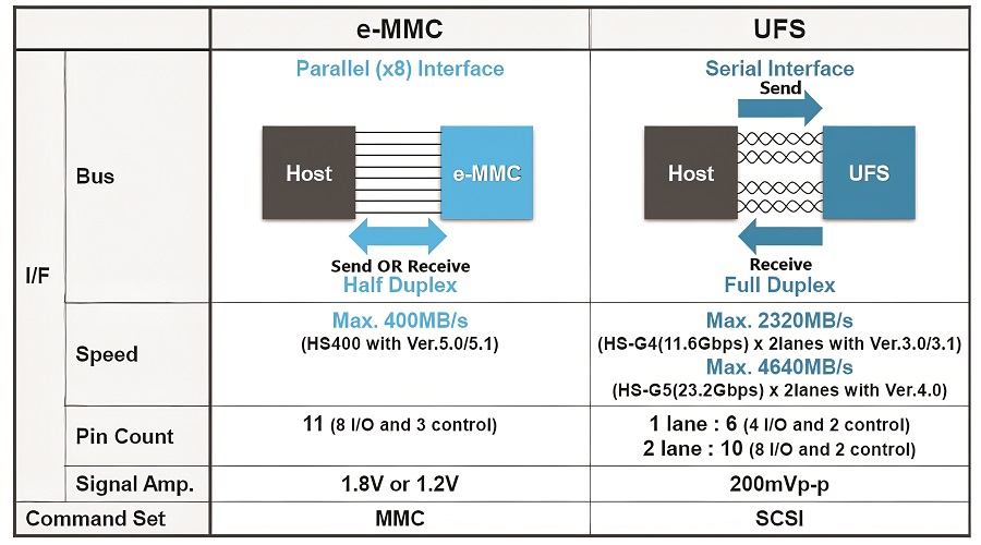
Standards such as Embedded Multimedia Card (eMMC) and universal flash storage (UFS) are evolving for memory storage in automotive applications.
UFS is the successor to the eMMC storage standard. Both eMMC and UFS are JEDEC-standard specifications, with a key feature being the integration of flash memory and a controller in a single package.
In 2013, eMMC devices started shipping for automotive use, with UFS following in 2017. Today, eMMC, which became a standard in 2007, is still used in many consumer, industrial and automotive devices. However, the transfer speed of eMMC is limited to 400 Mbit/s due to its parallel interface, which has increasingly led to eMMC being unable to keep up with high-end smartphones and other devices requiring faster operating speeds.
In 2011, the UFS standard was introduced, which uses a serial interface. Because the interface supports full-duplex communication, the host device can read and write data to the storage medium simultaneously. This has enabled transfer speeds to be increased significantly over those of eMMC, with UFS 3.1 (released in 2020) topping out at 2320 Mbit/s, and the most recent UFS 4.0 version achieving maximum transfer speeds of 4640 Mbit/s.
Limits of eMMC
NAND-based SSDs are finding adoption at the top-end of data-storage capacities over 1 TB in applications, such as ADAS L5 logging and sensor-fusion applications. At the lower end (32-256 GB) of the storage spectrum, eMMC has been the traditional medium. However, eMMC can no longer keep pace with the steeply evolving requirements of the latest systems.
Besides the need for large capacity, these huge blocks of data will need to be moved continually between the host processor and flash device. The interface bandwidth between them can act as a bottleneck or enabler of efficient transfer.
With a maximum capacity of 256 GB and a maximum data rate of 400 Mbit/s, traditional, eMMC-based media is highly limited in its applicability. Instead, the UFS standard offers storage capacities of up to 1 TB. The standardisation bodies (JEDEC and MIPI) have been evolving the data rates and capabilities of the UFS standard over the last decade.
The current UFS 3.0 devices can go up to 2.9 Gbit/s with two lanes. Given that the interface is bidirectional, this provides six times the speed possible over eMMC. This data rate exceeds that of 5 G transfers (2.5 Gbit/s), allowing for a smaller internal memory inside the host processor when data is being transferred between the flash device and external systems beyond the host processor.

It isn’t just the interface speed, but also the flash write speeds that are evolving. JEDEC enhanced write performance by introducing the write-booster feature in UFS 3.1, which adds a small pseudo SLC cache in the flash devices for easy, repeated access.
In terms of noise management, UFS improves on eMMC. Unlike eMMC, which is single-ended, the UFS interface is differential, making the system more resilient to transmission errors and noise, implying lesser probability of incorrect data interpretation and/or need for retransmission. The differential signalling also improves EMI performance, making it easier to pass automotive EMC standard CISPR 25 at system level.
Automotive storage is at a far higher risk of damage than consumer-grade variants. UFS lowers the overall risk of wear and tear of the storage device by allowing it to notify the host about large temperature variations. When the storage device indicates an alarming temperature, the host can throttle down or take action to cool it.
Low power operation is a mandatory requirement for electronics to reduce the carbon footprint and extend the battery lifecycle. UFS achieves this through differential signalling and an ability to switch to deep sleep mode.
UFS 4.0
UFS adoption began with smartphones but has spread to automotive applications. The mainstream for Level 3 vehicles has been storage that complies with UFS 3.1, but many automotive manufacturers are considering adopting UFS 4.0 in preparation for future vehicles that will require high-speed data transfers.
The UFS serial interface makes use of the MIPI Alliance’s M-PHY standard for its physical layer, and the UniPro protocol for its M-PHY interface.
The latest UFS 4.0 devices achieve speeds of up to 4000 Mbit/s and 2000 Mbit/s for reading and writing, respectively. Read performance is about twice that of the previous generation UFS 3.1 devices. This comes from the increased performance of the flash memory itself and its controller technology, which is in the same package.
The controller plays a crucial role in realising optimum flash-memory performance, and enabling storage products that come close to the maximum figures defined under UFS and other standards.
The controller is responsible for the fine-grained control and management of flash memory, and it is one of the most important determinants of storage performance. Developing a controller for high-performance storage is not feasible without extensive knowledge of flash memory.
The controller technology was particularly effective in accomplishing the maximum write speeds of 2000 Mbit/s by using a clever sequencing.
In addition to supporting HS-LSS (high-speed link startup sequence) to allow the system to start rapidly, UFS 4.0 memory devices include diagnostic functions to check their operating history, and functions to refresh and maintain the reliability of degraded data.
This enables the Link Startup defined in the M-PHY and UniPro initialisation sequence between the device and host to be performed at a faster HS-G1 Rate A of 1.248 Gbit/s than that of conventional UFS 3.0, at 3-9 Mbit/s. This is expected to reduce the time for Link Startup by about 70%, compared with the conventional method, to provide a faster boot time.
The refresh improves data reliability by refreshing degraded data to prevent corruption, even in the harsh, demanding in-vehicle environment. Extended diagnosis lets developers view important information from the UFS device, allowing preventative action to be taken.
The UFS devices have capacities of 128 GB, 256 GB and 512 GB. A technology called WriteBooster enhances write performance by using the existing user data area as a temporary single-level cell (SLC) buffer without sacrificing capacity.
This means the maximum SLC buffer size can be configured by the host at device configuration and the host can keep writing data to the buffer until it is full. This feature is enabled dynamically during operation by the host, depending on the system performance requirements of 5G and other applications.

UFS security
Security has become a key focus in automotive, given the risk it presents to human and asset life. As external connectivity penetration grows in cars, so does the security attack surface.
A hacker could send fake messages and cause trouble to in-vehicle communications. Examples include enabling/disabling the car, displaying incorrect navigation information, turning lights on/off, distracting the driver with audio, generating false dashboard alerts or taking complete control of the car.
These threats make the placement of security mechanisms imperative in system design. JEDEC, the standards body for UFS, has introduced support for inline encryption to prevent eavesdropping and man-in-the-middle attacks native to the specification.
Robust encryption mechanisms are proposed to allow for standardisation across host and device combinations. Encryption scheme support is a key differentiator between UFS and eMMC, making the former more appropriate for ADAS and black-box implementations.
Solid-state drives
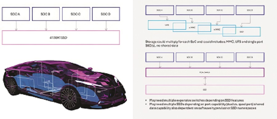
One of the key trends for data storage is the demand to support multiple system-on-chip devices. Rather than each chip having its own storage, and data having to be copied from one memory to another, a multi-port memory can support up to four devices. This avoids having to synchronise data across four different memory subsystems, which takes bandwidth and power consumption, and can cause errors.
The first SSD with four interfaces is designed to link to four system-on-chip (SoCs) devices to centralise storage for intelligent vehicles. This will better enable multitasking and centralising of automotive architectures, which are increasingly critical as today’s software-defined vehicles work across multiple SoCs and virtual machines to handle diverse workloads across in-vehicle infotainment (IVI) to ADAS and AI-enabled cabin experiences.
As most automotive storage drives can only connect to one SoC, they tend to either get placed locally with each system, leading to inefficient use of bits and space, or require the use of an expensive PCIe switch.
An alternative approach for sharing storage across SoCs relies on a costly, automotive-grade PCIe switch to connect a storage drive to multiple SoCs. These are often power-hungry and eat up valuable board space. The multi-port capability eliminates the need for a switch, giving carmakers more design flexibility in their vehicle while reducing heat and power consumption in the design.
The ability to connect multiple SoCs also alleviates the need to keep redundant copies of data, and the savings can be significant. For example, navigational data for a single city alone can be up to 100 GB, and it is often shared by ADAS and IVI systems, but existing approaches require this data to be stored at least twice within the vehicle, with local storage tied to each SoC. Multiply that by however many cities and that is hundreds of unnecessary gigabytes of storage.
The key to the quad-port SSD is a single-root input/output virtualisation (SR-IOV). This SR-IOV capability provides high performance for heavy, multi-host workloads of up to 64 virtual machines (VMs) to give each SoC and its VMs an isolated storage region for local processing, while sharing a pool of storage, maximising efficiency.
This support for multi-host workloads is essential as today’s automotive SoCs increasingly use VMs to multitask across different functions, from autonomous driving to vehicle-to-vehicle communication.
The SR-IOV capability offers an advantage by directing input/outputs (I/Os) directly from the VMs to the SSD hardware, contrasting with typical paravirtualisation, where I/Os are routed through a software hypervisor to the SSD, creating latency. By bypassing the software layer, the drive improves the random read performance by a factor of three.
Virtualisation also enables increased security for carmakers. Based on the SR-IOV virtualisation, the data of each VM is isolated from others in the hardware to mitigate data or code leakage while curtailing hacking attempts in one VM from compromising another, thus maintaining critical data privacy and security.

The quad ports provide multiple independent data paths, allowing concurrent communication with the host system. They can be allocated to different VMs or workloads, ensuring strict isolation of data traffic to separate latency-sensitive applications or high-throughput workloads.
Each VM can have its own isolated storage region, or namespace, to store and access data, while sharing a pool of data with others. System architects can selectively allocate ports, ensuring critical data remains isolated while allowing efficient data sharing when needed. Private namespaces, combined with SR-IOV, ensure data can only be accessed by the virtual machine or host attached to the namespace, maintaining critical data privacy and security.
The SR-IOV capability is combined with a PCIe Generation 4 interface and ruggedised automotive design, with random read and write speeds above 600,000 I/O operations per second (IOPS) and above 100,000 IOPS, respectively, for a 4 KB transfer. This allows the drive to efficiently manage data streams from multiple SoCs at once.
For example, an automotive OEM can connect one port to an ADAS system and another to an IVI system, allowing each to store private data while accessing a common set of critical map data and reduce the cost per gigabyte of storage. This boosts performance and dissolves bottlenecks as both can access shared data simultaneously, and it alleviates the need to keep redundant copies of data. The quad ports also reduce the need for extra storage devices.
As existing solutions can typically connect to only one SoC on their own, they tend to get placed locally with each automotive system, leading to unused capacity; alternatively, they require OEMs to use a costly, automotive-grade PCIe switch to connect a drive to multiple SoCs. By centralising storage for multiple systems, the SSD dramatically improves efficiency while streamlining architecture.
The SSD is built with its triple-level cell (TLC) NAND, but it can be configured to support SLC and high-endurance (HE-SLC) data endurance groups, which offer 20 times and 50 times the endurance of TLC, respectively, to meet unique data requirements.
For example, the HE-SLC endurance group can be used for heavy-write use cases, such as continuous black-box data recording, where cars must constantly rerecord critical data from sensors, cameras and Lidar. In such a scenario, where data is being programmed and erased every few minutes, the HE-SLC mode offers the required endurance while eliminating the need for more expensive, volatile memory, such as DRAM.
The SSD is designed to ASIL-B to support safety-system requirements, and it is offered in a ball-grid array package to help withstand the shock and vibrations typical of vehicles’ rugged environments, with capacities up to 1.8 TB to enable efficient storage of AI algorithms, large language models, advanced infotainment and telemetry data for the next generation of vehicles.
Again, security is key, and the SSD includes hardware-based data encryption, device attestation, secure boot and cryptographically signed firmware.

Conclusion
The evolution of AV design is having a major impact on data storage. The move to a centralised architecture presents opportunities for multi-port storage, saving on costs and wiring weight, but is a challenge for the speed of retrieval and capacities. While NOR memory supports code storage, the latest NAND memory technologies and UFS standards are driving storage for AI and sensor-fusion data forwards.
Acknowledgements
With thanks to LJ Chen and Mehak Kalra at Synopsys, Tetsuya Yamamoto at Kioxia and Barbara Kolbl at Micron.
UPCOMING EVENTS


