


Image sensors
Safety in numbers
A growing move to using arrays of less expensive sensors in autonomous systems is opening up new design options. Nick Flaherty explains the implications
One of the key tools for autonomous systems is the image sensor. To put that into perspective, about 30,000 people are killed on US freeways each year, and image sensor developers have the ambitious aim of reducing that to 300 using advanced driving assistance systems (ADAS). These automate the braking process using data from image sensors, driving up the volume and quality of the sensors produced, and driving down their cost.
These less expensive sensors, coupled with the development of machine learning (ML) algorithms tuned to image sensors for an ADAS, are also being applied to uncrewed system designs.
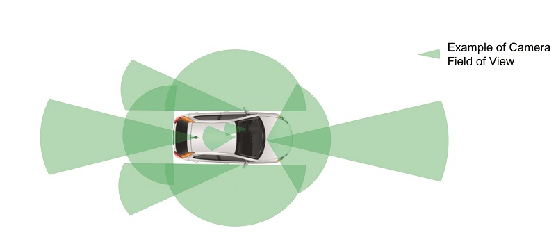
This is a key route to making self-driving vehicles more affordable to build, and is changing the way autonomous vehicle sensor systems are being designed. Instead of one large, expensive sensor to capture a wide field of view, research projects for L5 self-driving vehicles are showing that using an array of smaller, lower-cost sensors is practical, tapping into the existing ecosystem of AI algorithms.
This array approach also gives a product designer more options. The driverless cars used for research have large sensor hubs protruding from the vehicle to house a wide range of sensors including the image sensor, Lidar and radar. As the technology moves to mass adoption, the multiple sensors will need to be integrated into the body of the vehicle, and styling becomes as important a design factor as the integration with the rest of the electronics in it.
Lens
This shift to the styling requirements has a major impact on lens technology. The pixel technology stays roughly the same as for the ADAS sensors, but there is demand for more pixels in the sensor array, going up from 8 MP now to 12 MP to give higher resolution.
A higher resolution allows smaller objects to be detected at a greater distance, giving more time for the ML algorithms to make an identification and allowing the self-driving system to operate safely at higher speeds. There is no set ‘perfect’ resolution, though – the required resolution is measured against specific use cases that address specific problems such as detecting a certain size of obstruction at a certain speed or distance.
However, this higher resolution in turn requires a larger lens, which increases the size of the camera. At the same time, there is demand from vehicle designers for a smaller lens, of 0.25 in or so, to fit in with the styling, rather than the current 0.5 in.
That creates a challenge for the light-gathering capabilities, as less light is captured through a smaller lens. That in turn drives demand for sensor arrays with larger, more sensitive pixels, leading to a more expensive sensor or reducing the resolution with fewer pixels.
That trade-off between higher resolution and larger pixels is still being explored, using sensitivity as a metric, where the challenge is to shrink the pixel size but keep the low-light performance. The key here is ensuring a large enough dynamic range, as the pixel has to avoid becoming saturated in bright light yet still be sensitive to low light.
Current high-volume image sensors for ADAS have a resolution of 8.3 MP using 2.1 µm2 pixels. These are increasing in volume shipments as cameras on the windshield for ADAS Level 3 systems, and are now being used for L4 and L5 applications as an array. The arrays can be rectangular, for example 12 sensors in a 4 x 3 array, each with their own lens, or a ‘belt’ of sensors in a 12 x 1 array to give 360o visibility.
Shutters
The move to reduce costs also has an impact on the type of shutter used. Rolling shutters, where the image is acquired row by row, is more cost-effective than global shutter technology, which reads every row simultaneously into a memory buffer. The increase in performance of the pixel readout means rolling shutter sensors are now fast enough to be used with ML processing, where the ML algorithm is trained specifically using the output of the rolling shutter sensor.
With a rolling shutter the sensor data is read out row by row, so additional memory is not required in the sensor, reducing the cost. However, that means the top rows of the sensor image are sensing light before the bottom ones, so a vertical post or stop sign can appear tilted. ML networks are a way to compensate for that though, by mapping the original image to the output of the sensor to compensate for the blur.
Fast motion can result in blurring as a result of using a rolling shutter, but higher performance ML algorithms can increasingly compensate for this. A rolling shutter also allows multiple exposures to be combined into a single image.
That improves the dynamic range and provides more metadata about the image that can be used by the ML algorithms. For example, the metadata can include the exposure data of specific areas of the image, with automatic white balance and a feedback loop for exposure control all implemented on the sensor chip.
Taking one exposure from the sensor array currently provides 110 dB of dynamic range, but combining three or four exposures on the sensor can provide a range of 140 dB, rather than having to send multiple images from the sensor. That helps to cut the sensor’s bandwidth requirements, and performing the calculations on the sensor rather than in the AI chip helps to reduce the overall power consumption of the sensor system.
The higher dynamic range is particularly important for situations such as detecting backlit traffic lights. If the pixel is approaching saturation it loses the ability to distinguish colours, particularly between yellow and red, so there is a benefit in increasing the dynamic range of a single frame by using multiple exposures.
The next stage is to reduce the number of exposures to two with the same
140 dB dynamic range, by improving the pixel’s design so that it can be exposed for longer to absorb more light before it saturates. The current leading-edge pixel designs provide a dynamic range of 130 dB from a single frame.

Improving the dynamic range will also help improve the efficiency and performance of future sensors when dealing with corner cases, those unusual situations that can confuse sensors when the vehicle emerges from a tunnel into bright light for example.
The current state-of-the-art 8.3 MP 0.5 in CMOS digital image sensor has an array of 3848 x 2168 pixels with either the on-chip high dynamic range multiple exposure approach or a linear exposure output for off-sensor processing.
The sensor also includes fault detection and embedded data that are designed to enable compliance with the ASIL B functional safety requirements. The device is programmable through a simple two−wire serial interface and supports the MIPI output interface.
Agricultural and construction
The cost reduction of sensor systems from consumer ADAS means the sensors are also being used in agricultural and construction equipment, taking advantage of the automotive temperature range of -40 to +85 oC.
In this application, vehicle styling is less important than its ruggedness and ability to withstand harsh environments, which opens up the opportunity for larger lens designs. There is also a different trade-off for the resolution, as the speed of the vehicles is much slower but smaller objects need to be detected.
Event-driven sensors
Another type of image sensor is the event-driven sensor (EVS). Instead of outputting all the pixels in the sensor array, an EVS outputs only those that register a change.
An EVS uses a different ML technique called spiking, or neuromorphic, neural networks that mimic the way the brain works. They have a lower power consumption and a faster response (lower latency) than a traditional CMOS sensor, as only the change beyond a set threshold, known as the temporal threshold, is registered.
However, EVSs are not suitable for the main camera in a driverless vehicle on their own, as at high speed all the pixels are changing, but they are finding uses as a secondary sensor alongside radar or Lidar that can quickly identify an area in the field of view for the main sensor to focus on.
Outside the vehicle, EVSs support automated electronic braking systems using the low latency and intrinsically high dynamic range of the technology. They also support scanning Lidar systems, which come with a resolution/accuracy trade-off by detecting multiple, arbitrarily shaped regions of interest on which a Lidar can focus its attention.
However, this is a new approach, and sensor manufacturers and Tier 1 suppliers need new system architectures in order to develop these use cases to a level of reliability and accuracy that meets automotive standards.
EVSs are also increasingly interesting for UAVs for camera-based collision detection systems as a result of the low power consumption and fast response, which reduces the battery payload required.
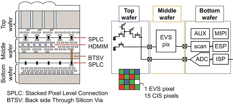
The latest EVS combines the pixel array, electronics and ML processing on three stacked wafers to achieve a high-performance, low-power system.
The key element in the design is the temporal contrast detection, which is a more complex algorithm than the processing currently used on image sensors. This is a relative measurement, and is encoded by ‘events’ – a combination of the x-y pixel location, event time stamp and the polarity – indicating whether an increase or decrease in illuminance has been detected.
Many applications require EVSs to be used alongside a traditional CMOS image sensor (CIS) to get absolute measurements of the illuminance. Dual-sensor configurations have several shortcomings though, such as the parallax error from the camera collocation, complexities in synchronisation, and the added cost from the need for two pairs of lenses and more complex packages.
An early hybrid EVS-CIS sensor uses the photocurrent (the current from the photodiode) for the time-continuous front-end circuit in the EVS, and then integrates the photocurrent on a sampling capacitor for the CIS. However, this approach is not easily scalable, as the CIS pixel pitch is limited by the EVS pixel pitch, which is far larger as a result of the larger pixel processing electronics.
Also, storing the charge from the pixel for EVSs does not benefit from the high image quality offered by the pin photodiode used in CIS sensors. Instead, wafer-level stacking technology can be used to achieve high-resolution EVS functionality without sacrificing CIS performance.
The top-layer wafer uses pin photodiode pixels arranged in a 4 x 4 configuration, forming a macro-pixel. Each macro-pixel substitutes one blue-channel CIS pixel for a clear one, which is usually connected to an EVS readout circuit on the middle wafer.
The photodiode is connected via a stacked pixel-level connection, giving an EVS pixel pitch of 8.8 µm, and the photocurrent is converted into a log voltage and fed into a filter amplifier that acts as the actual contrast detection circuit.
The filter amplifier also uses a programmable high-pass filter characteristic to avoid noise events driven by leakage currents that would otherwise discharge high-impedance nodes, leading to false event triggers.
A subsequent comparator stage detects if a contrast change above the programmed threshold has been detected. When an event is detected, an in-pixel latch stores it, and a 4-bit sample is produced from a ‘time-to-digital converter’ (TDC). This provides a faster and more robust readout than an analogue implementation.
The readout circuitry of the EVS pixel array is located on the third wafer and connected to the middle wafer by means of through-silicon vias. The CIS pixel array is read by analogue-to-digital converters that are also on the bottom wafer, alongside an event-signal processor (ESP), an image signal processor, a fast MIPI interface and auxiliary functions.

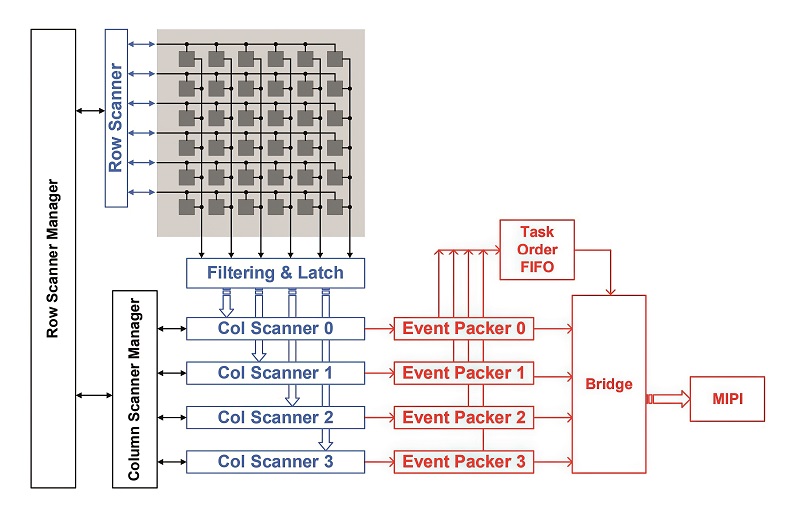
Combining the event-driven pixels with the image pixels give the lower power and lower latency. A row-pixel interface detects if at least one pixel in the array has detected an event and subsequently triggers a pulse to request a sample.
An asynchronous token-based readout then scans for the first row having an event using skip-logic to jump over rows that don’t have to be read. The skip-logic is implemented hierarchically to reduce the load on driving stages and buffers. If a row is found to have an event, a signal is sent back to the array and the column readout block.
Four parallel readout channels, each running at up to 250 MHz, provide a data throughput rate of 1 GEvent/s (GEPS) without having to drive the entire scanner with a 1 GHz clock, reducing the power consumption by a factor of eight.
The column readout samples all the information in the selected row and provides a signal to the row’s pixel interface indicating that a new sample pulse can be generated. If all the buffers are occupied, the scan has to be stopped to avoid data loss. That can introduce excess latency though, which is why the in-pixel TDC approach is used.
The column readout incorporates similar skip-logic to the row selective scanner. The sensor uses a conventional off-pixel time-stamp assignment, where the scanner can detect in parallel if neighbouring pixels share the same polarity.
That means only the outermost pixels need to be encoded, reducing the scan and MIPI interface bandwidths, so that a maximum event rate of 4.6 GEPS is achieved.
The ESP processing block provides essential functionality such as region-of-interest control, defect pixel correction, event rate limitation, event encoding and caching for the MIPI interface. It also provides auxiliary functions such as ambient light level sensing (ALS) and activity monitoring (AM). The ALS essentially samples the summed photocurrent of all the event pixels by measuring the local current.
An event-rate limiter drops events above predefined, programmable thresholds to avoid false triggers. Up to three activity-based thresholds are supported, and are selected in real time based on the AM block.
AI integration
For computationally intensive applications such as rolling-shutter correction, deblur or slow motion from video frame interpolation, developers need to use the latest neural processor units (NPUs) built in advanced process nodes such as 3 nm CMOS to give the maximum performance and compatibility with software frameworks, rather than the more mature processes used to make image sensors.
While it might be possible to use a different, leading-edge wafer technology in a stacked wafer, it is a much more difficult process for building the stack, and risks raising issues with reliability. Instead, the MIPI interface is used to connect to the NPU for processing.
Interconnection
For the connection to local processing over a distance of 10 cm, MIPI works well, and it is an industry standard. Connections beyond 10 cm though require a serialiser/deserialiser (SerDes) interface, and there are two specifications for this that are not compatible.
It means that the SerDes interface for the vehicle’s ECU has to be used by the sensor, reducing the ability of system designers to use sensors from different suppliers; also, a camera might need to be redesigned to work with a different ECU. Industry is currently pushing to create a single standard for SerDes connections, but that will limit the integration of SerDes into the sensor, requiring additional SerDes chips.
MIPI
The latest version of the MIPI camera system interface (CSI), MIPI CSI-2 v4.0.1, was agreed in November 2022 and uses several of the MIPI physical layer (PHY) standards. This protocol specification provides selectable data rates from 1.25 Gbit/s up to 5.8 Gbit/s, with different clock speeds to avoid EMI problems.
The v4.0 specification adds an advanced ‘always-on’ imaging solution that operates over as few as two wires to lower the cost and complexity, reducing the size and weight of UAV camera systems. It also adds multi-pixel compression for the latest generation of advanced image sensors and RAW28 colour depth to provide higher image quality and signal-to-noise ratio.
The MIPI CSI protocol is typically implemented for shorter-reach applications on either a MIPI C-PHY or MIPI D-PHY interface – v4.0 is the first to support transmission of CSI-2 image frames over the low-cost, low-pin-count MIPI I3C/I3C Basic two-wire interface.

However, a key advantage of CSI-2 v4.0 is that it is backward-compatible with all previous versions of the MIPI specification.
CSI-2 v4.0 includes an Always-On Sentinel Conduit (AOSC) that enables the development of always-on machine vision systems, where the image sensor and video signal processor (VSP) can continuously monitor their surrounding environments and then wake their more powerful host CPUs only when significant events happen. Typically, the VSP will be either a separate device or integrated with the host CPU within a larger SoC.
AOSC enables image frames to be economically streamed from an image sensor to a VSP over a low-power MIPI I3C bus in a highly efficient manner, with scaling options to add extra I3C lanes and bandwidth as defined by the I3C specification.
In addition, Multi-Pixel Compression (MPC) provides optimised pixel compression for the latest generation of CMOS image sensors with multi-pixel colour filter arrays. It helps alleviate the high bandwidth demands of the sensors by compressing both multi-pixel and standard images more efficiently and with potentially higher quality than current methods. Reference code has also been made available to help integrators evaluate the algorithm and verify their implementations.
RAW28 pixel encoding supports the high dynamic range automotive image sensors for ADAS and autonomous vehicle designs.
SerDes
The MIPI CSI-2 protocol can also be implemented over the MIPI A-PHY long-reach SerDes interface (up to 15 m) for use in applications such as automotive ADAS, but there are other options for this longer reach.
The Automotive SerDes Alliance (ASA) gave the first public demonstration of its Motion Link (ASA ML) SerDes technology in November 2022. The technology was part of a proof of concept developed by BMW that connected several cameras and displays via an Ethernet backbone, while using either the ASA ML technology or IEEE 802.3ch multi-gigabit Ethernet for the asymmetric high-speed comms.
The first version of the ASA protocol runs at up to 16 Gbit/s, while the next version is aiming at 42 Gbit/s to transfer the raw camera data rather than having the processing done in the sensor.
Integrating multiple standardised high-speed technologies into a single Ethernet network for applications, rather than using proprietary point-to-point connectivity, allows the development of true zonal architectures for driverless cars with the reuse of sensor data in multiple computing units with the latest high-performance ML NPUs.

Conclusion
Image sensors are a complex combination of pixel technologies, on-chip processing and interconnections that is constantly evolving. Adding event-driven sensing to traditional CMOS image sensor arrays can reduce power consumption and latency to boost the performance of sensors for vehicles and UAVs. At the same time, the evolving SerDes standards are allowing the sensors to be connected in new ways and linked to high-performance NPUs to implement the ML algorithms.
Acknowledgements
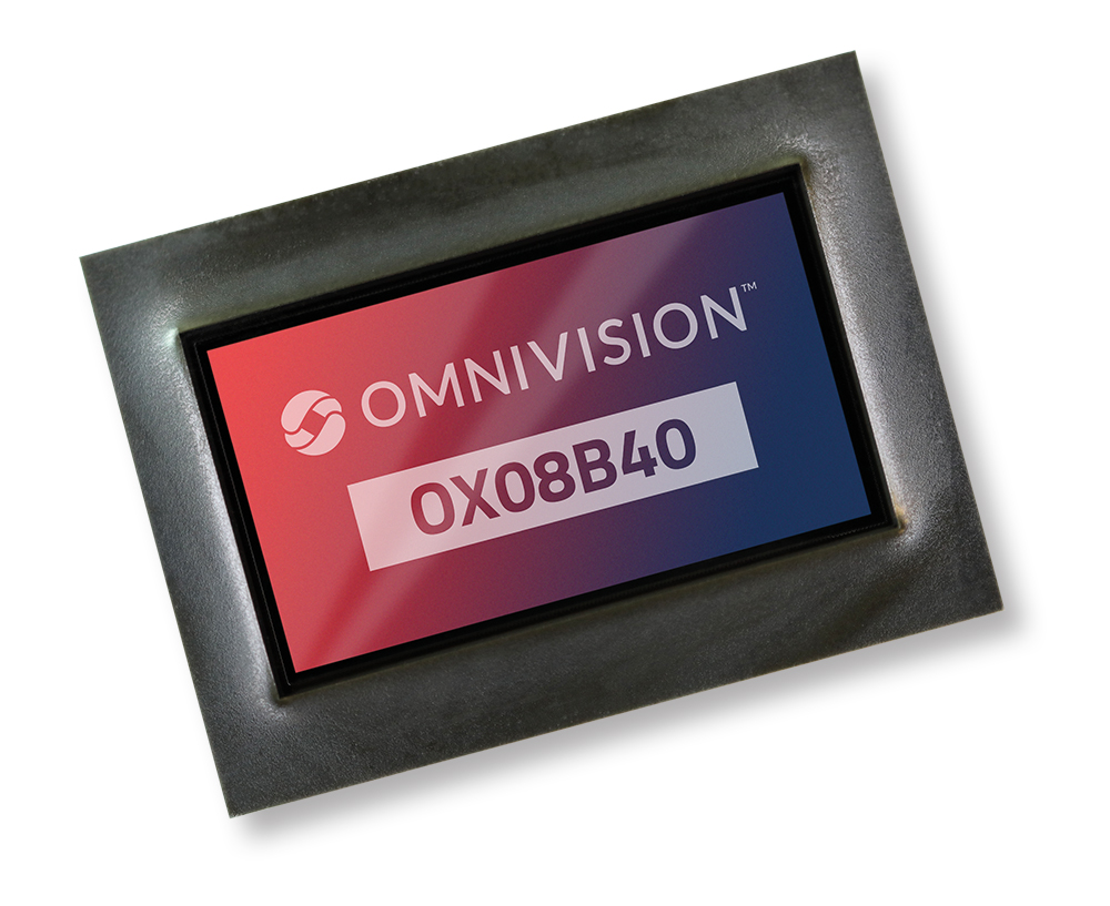
The author would like to thank Geoff Bellows at onsemi and Andreas Suess at Omnivision for their help with researching this article.
UPCOMING EVENTS


