


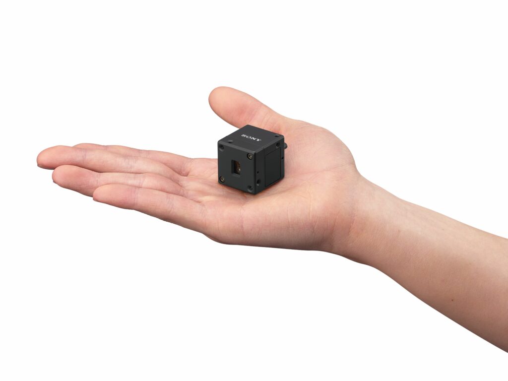
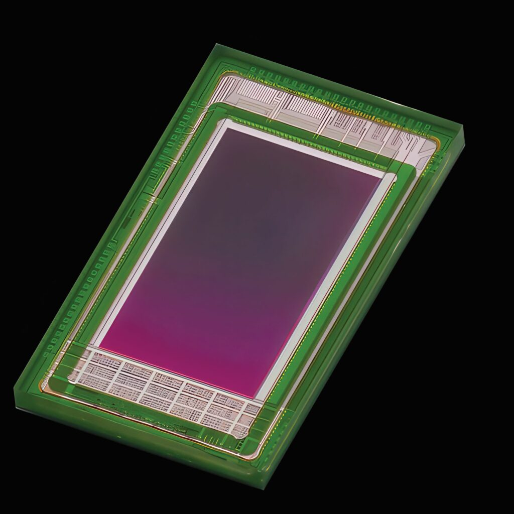
Image sensors
(Image: Sony Semiconductor)
Small and sensitive
Nick Flaherty reveals the latest advancements in image sensor technology
The advancement of uncrewed systems is inextricably linked to the evolution of image sensors. These range from higher-resolution sensors for visual navigations systems, to 2D, 3D and even 5D sensors with time-of-flight (ToF) sensing for AGVs, and then to the latest infrared sensors into the long waveband. There are also new 2D materials and quantum dot (QD) technologies that boost sensor performance.
Visual navigation
A visual navigation system (VNS) uses onboard cameras to capture real-time environmental imagery that enables autonomous platforms in the air and on the ground to calculate precise movement, recognise landmarks and build 3D maps without GNSS satellite data. It reduces inertial drift error to under 1% by constantly correcting high-frequency IMU data with measurement data.
The key requirement is not raw pixel count, but image consistency, sufficient texture and stable contrast to support robust feature extraction across changing environments.
To address natural fluctuations in illumination, contrast and scene appearance, a VNS relies on advanced image-processing and AI-based algorithms. These algorithms dynamically compensate for variations caused by lighting changes, shadows, motion blur or terrain appearance by normalising image data and focusing on persistent visual features rather than absolute brightness values. This allows the navigation solution to remain stable across different times of day, weather conditions and surface types.
From an operational standpoint, the effective navigation range is therefore not defined by a fixed distance or altitude, but by the availability of meaningful visual features within the camera’s field of view. In practical terms, this means the VNS supports navigation from low to medium altitudes, where sufficient ground texture is present, complementing the inertial navigation system by continuously correcting drift rather than acting as a standalone positioning sensor.
By design, the VNS works as part of a sensor-fusion architecture within the autopilot, combining visual information with inertial data. This ensures that navigation performance gracefully adapts to changes in altitude and operating conditions, maintaining reliable position estimation in GNSS-denied environments without imposing restrictive altitude envelopes.
The image sensor uses a global shutter to avoid image distortion caused by platform motion and vibrations. Unlike a rolling shutter, the global shutter captures the entire image simultaneously, which is essential for preserving geometric consistency and ensuring reliable feature extraction for visual navigation in dynamic flight conditions.
Beyond basic image quality characteristics such as resolution and dynamic range, several system-level factors must be considered when selecting and integrating an image sensor for visual navigation. These include latency, synchronisation, robustness to vibration and motion, power consumption, environmental tolerance and long-term reliability under operational conditions.
The VNS has been optimised to process image data efficiently while maintaining deterministic control loops. Rather than storing or processing full images continuously, the system extracts and retains only relevant points of interest, which are used for navigation and mapping purposes. This approach significantly reduces data volume, memory usage and computational load.
Equally important is how the image sensor fits into the overall avionics architecture, rather than being treated as a standalone component. In the case of the VNS, the sensor is tightly integrated with the autopilot, which provides precise timing, synchronisation with inertial measurements and deterministic data handling. This ensures that visual information can be accurately fused with inertial data in real time, which is critical for stable navigation performance.
Designing the VNS as part of a fully integrated guidance, navigation and control ecosystem ensures that image-based navigation is not limited by sensor characteristics alone, and benefits from a robust autopilot architecture that maximises reliability, scalability and mission adaptability.
Time of flight
Another way that image sensors boost the accuracy of operation of uncrewed aircraft is using direct ToF (dToF) sensing.
The dToF technology provides fast and accurate measurement, distance resolution and measuring range in the world’s smallest and lightest image and depth sensor. One such module measures just 29 mm x 29 mm x 31 mm (approximately 1.14 in width x 1.14 in height x 1.22 in depth), excluding protrusions, and weighs only 50 g for UAVs and autonomous robotics.
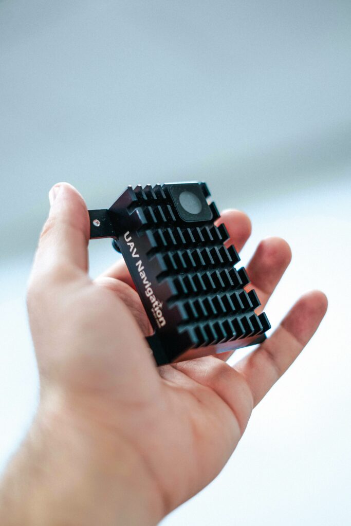
(Image: UAV Navigation-Grupo Oesía)
The module has a single-photon avalanche diode (SPAD) sensor that provides multiple ranging points for distance measurement and can accurately measure distances in three dimensions: length, width and depth.
The sensor can even measure distances to low-contrast subjects and objects with low reflectivity, which are more difficult to detect with other ranging methods. This enables accurate measurement of distances even in environments such as retail stores, where various objects, including people and fixtures, are expected.
In addition to its ability to accurately measure distances both indoors and outdoors, the sensor’s lightweight design and rigid aluminium housing allows for integration into autonomous mobile robots in warehouses and into UGVs used for inspections and surveys.
The dToF ranging module, equipped with a SPAD sensor, achieves highly accurate measurements and distance resolution. It can measure at various distances, for example at 10 m (approximately 32 ft) with a margin of ±5 cm (nearly 2 in) both indoors and outdoors.
(Image: Sony Semiconductor)
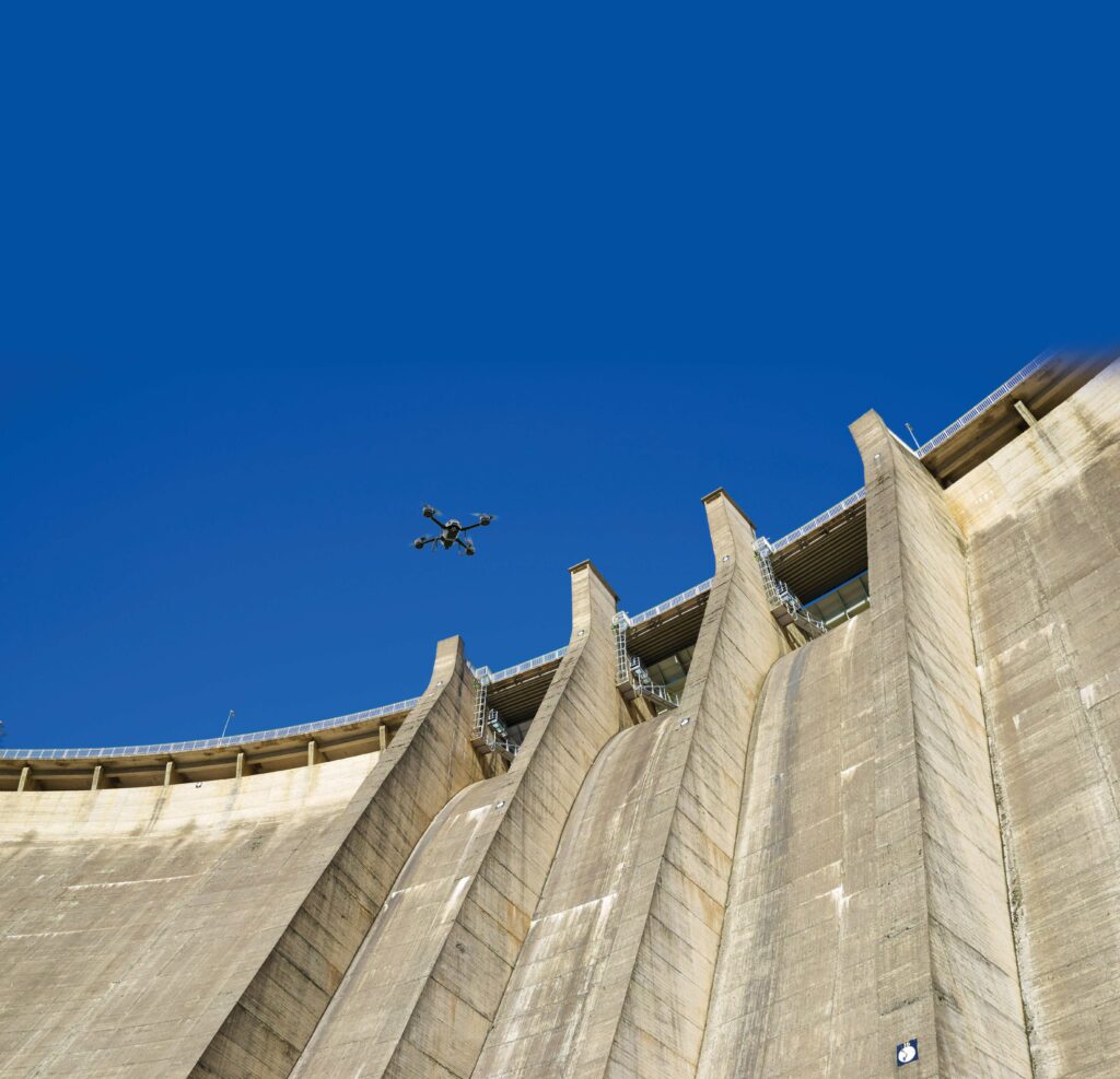
It is also capable of accurately measuring distances to various objects that are difficult to detect with other ranging methods. This includes low-contrast subjects, objects with low reflectivity and floating objects. It is highly accurate even at long distances of 40 m (approximately 131 ft) indoors and 20 m outdoors under bright summer conditions (assuming 100,000 lux), which can be challenging when inspecting infrastructure such as bridges, highways and dams.
2D sensors
2D sensors are designed for high-performance imaging where spatial resolution and high frame rates are paramount.
Global shutter technology is key. As mentioned, unlike standard rolling shutters that cause distortion during high-speed flight, these sensors use global shutters to capture the entire frame simultaneously. This is essential for UAVs and driverless vehicles traveling at high speeds.
.jpg)
Many of these sensors are optimised for the near-infrared spectrum, allowing UAVs to operate during twilight or in poor weather conditions when visible light is insufficient.
The shift toward fully autonomous UAVs has necessitated the development of 3D sensing, which combines ToF technology in the 2D array. These ToF sensors measure the time it takes for a light pulse to bounce off an object and return to the sensor while a three-pixel architecture allows for fast transfer times (down to 10 ns) and eliminates motion artifacts.
3D sensors act as the ‘eyes’ for detect-and-avoid systems, allowing UAVs to navigate complex environments like forests or urban canyons. By generating real-time depth maps, UAVs can identify safe landing zones and navigate to docking stations with centimetre-level accuracy.
A key feature of 3D image sensor technology is its ability to operate alongside other active 3D systems without interference. This is crucial for ‘swarm’ UAV operations where multiple drones are sensing the same space.
The most recent innovation is a sensor that provides both high-speed 2D grayscale data and 3D depth maps simultaneously from a single CMOS silicon chip.
This combines a small 2.5 µm global shutter pixel with a post-processing diffraction layer to create angular sensitive pixels. This enables 3D angular signal raw data to be generated and then processed by a compatible software development kit. A 2 megapixel (1920 x 1080) full HD-resolution sensor is currently available in both monochrome and colour with a form factor of 7.65 mm x 4.45 mm (approximately 0.30 in x 0.18 in) that makes it easy to integrate into space-constrained optical engines or modules. It uses 200 mW of power to run at full frame rate, and generates 3D depth maps and displays the contrast details of any kind of object – even black or very shiny ones, or those seen through sheets of glass or transparent organic material such as plexiglass or plastic bottles.

Unlike other 3D technologies, which rely on illumination of the scene, the sensor can be used in very diverse operating conditions, including indoor lighting or direct sunlight. Compared with a stereoscopic solution, only a single sensor plus a lens is required, without the need for complex dual-lens system alignment and there is no risk of optical occlusion.
By fusing the 2D and 3D data into a single stream, UAV manufacturers can reduce the weight and power consumption of the payload – a critical factor in extending flight time. This ‘hybrid’ approach is currently being used for indoor warehouse UAVs and last-mile delivery robots, where the sensor must identify a package (2D) while navigating around obstacles (3D) in a single, time-aligned frame.
Infrared
Infrared image sensors are a key technology for uncrewed systems. Unlike thermal infrared, which detects heat emitted by objects, infrared behaves more like visible light because it is reflected by surfaces. However, because its wavelengths are longer than those of visible light, it can penetrate atmospheric obstacles such as fog, haze and smoke that would otherwise blind standard cameras.
SWIR
Short wavelength infrared (SWIR) covers the wavelengths between 0.9 and 1.7 µm (and sometimes extending to 2.5 µm). Many materials have unique spectral signatures in the SWIR band. UAVs use this spectrum for agricultural monitoring (detecting plant moisture stress) and mineral exploration, identifying substances that look identical to the naked eye.
SWIR sensors also take advantage of night airglow – a faint light emitted by the upper atmosphere. This allows UAVs to capture clear, high-resolution images in near-total darkness without the need for active illumination.
(Image: Teledyne e2v)
Because SWIR sensors use reflected light, the resulting images have shadows and contrast similar to black-and-white photos, making them much easier for human operators or AI algorithms to interpret compared with blurry thermal ‘blobs’.
Colloidal QDs (CQDs) can be monolithically integrated with the readout circuit, enabling high resolution and high pixel density. With a tunable bandgap, they can extend the functionality of CMOS image sensors beyond the silicon cut-off wavelength into the shortwave and mid-wave infrared regions, and support multispectral architectures and low-noise pixel designs.

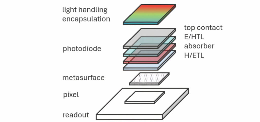
Image sensors using thin-film photoactive layers should be seen as a new technology platform that can be customised depending on the application. A stack of materials (each with submicron thickness) is built monolithically on top of the readout circuit, which can be based on CMOS or a thin-film transistor.
Each stack contains the absorber layer, which can be CQDs, built with organic polymers or small molecules, or a perovskite material. This layer is sandwiched between electron transport layers and hole transport layers, and their order defines the polarity of the photodiode.
Additional layers such as light manipulating ones (such as metasurfaces below or filters above) or encapsulation can be further added to adjust specific features.
The photodiode and pixel can be tuned largely separately, and the spatial metrics (such as pixel size or resolution) are defined only by the underlying readout technology.
Most previous implementations of CQD sensors have used lead sulphide as the absorber material. This has shown external quantum efficiency (EQE) of above 80% at 1400 nm, pixel size below 2 μm for high-resolution sensors fabricated on 300 mm wafers for 6 Mpixel sensors or extended SWIR functionality up to 2 μm wavelength.

Rather than lead, the most notable contender for the absorber seems to be indium arsenide, which is promising with a higher sub-nanosecond response speed and better reliability. There continues to be rapid progress on improving the EQE, with a value of 79% reported at 940 nm, and results that cross the barrier of 30% EQE at 1250 nm for top-illuminated stacks on a silicon substrate, compatible with integration with the readout circuit. Dark current density is still under improvement, with 30 μA/cm2 at -3 V bias for these initial devices. Other candidates being investigated are indium antimonide (especially for cut-off wavelength extension), silver telluride with a recent imager proof-of-concept demonstration and mercury telluride, which is interesting for the mid-wave infrared (MWIR) range but is not RoHS compatible.
Initial demonstrations of QD-based image sensors have one stack covering the entire focal plane array (FPA), which means that all pixels have the same spectral response. This also means that the resulting imager has a broadband response because QDs show sensitivity throughout the bulk visible range, extended all the way to the silicon cut-off, which is defined by the nanocrystal size.
There are several approaches to create wavelength band distinctions per region or per pixel. These include stacking QDs of different size, side-by-side QD stacks or filters on top of the stack. A new approach is based on metasurfaces fabricated as a part of the standard back end of line fabrication process.
In this way, each pixel of the array can have a dedicated wavelength response by tuning the effective refractive index with a scalable design of the flat optics element under the QD pixel stack. In this ‘multispectral-by-design’ concept, the peak response can be adjusted by altering one process module according to the requirements of the application, and by keeping a single QD stack everywhere.
As a result, CQDs should be seen as an enabler for realisation of a new image sensor platform. With monolithic, wafer-level integration of thin-film photodiode stacks on readout, cost in mass production can approach single-digit values. This could dramatically lower the barrier for implementation of infrared imaging. Ongoing developments on lead-free stacks, low-noise 4T pixels and metasurface-based multispectral-by-design arrays show the path forward toward customisable imagers.
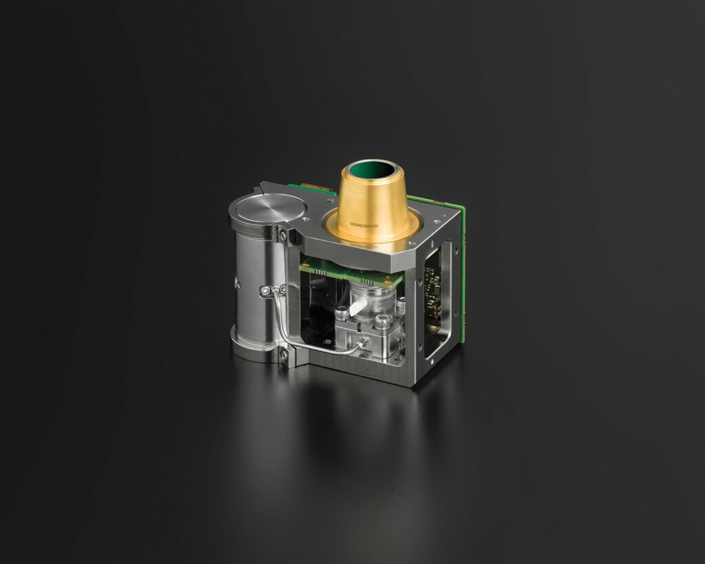
Mid-wave infrared
(Image: imec / Malinowski et al)
MWIR sensing is also reducing in size and weight for UAVs with a VGA module that measures 56 mm x 77 mm x 73 mm (approximately 2.02 in x 3.03 in x 2.87 in) and weighs 360 g.
Thermal imaging is no longer a complementary sensor in such scenarios– it is a decisive capability. In harsh conditions such as cold weather, rain or fog, or in complete absence of light, MWIR sensing provides reliable detection and identification where visible cameras fail.
MWIR sensors reconcile full-band MWIR performance with a compact SWaP high-operating-temperature architecture. The module integrates a type II superlattice (T2SL) FPA, operates at 130 K and covers the full MWIR band from 3.7 to 4.8 µm. This extends the visibility from existing MWIR sensors that cover the blue band between 3.6 and 4.2 µm. While the MWIR blue band delivers the highest detection range with the lowest power consumption, the extended spectral coverage offered by the MWIR red band enhances the signal-to-noise ratio and improves image quality in challenging environments.
From an integrator’s perspective, the latest MWIR sensor provides VGA resolution at 640 x 512 pixels with a 15 µm pixel pitch, while maintaining power consumption at 4 W dc. A compact module format is compatible with sub 6 in gimbals for tactical UAVs, and can also be deployed in handheld or soldier-worn systems.

Beyond raw performance, integration speed has become a strategic differentiator. Development cycles are shortening and OEMs seek modular architectures that limit redesign efforts. Standardised interfaces streamline integration of cooled detectors. This simplifies product integration into OEM cameras, shortens time to market and enhances overall system reliability by using a split linear cooler.
An advanced thermal imager version adds image correction functions such as non-uniformity correction, bad pixel replacement, denoising, destriping and colour mapping. This further accelerates system-level integration and reduces software development overhead for customers.
Long wavelength
A type II lattice can also be used for long wavelength image sensing. An indium arsenide/gallium antimonide-based longwave superlattice structure has been redesigned for optimal photon absorbance, barrier performance for low dark current and enhanced operability. The superlattice structure was processed into a 640 x 512, pixel pitch 15 μm FPA with a long wavelength ranging approximately from 7.3–9.6 μm, with simultaneous readout mode. Both dry etching and passivation for the detector devices were optimised during the process to achieve high-quality disk mesa. After being flip-chip bonded with customised read-out integrated circuits, the noise equivalent temperature difference of the FPAs were measured as 25.3 mK, with response non-uniformity of 3.48%. The detectors presented high-quality infrared images with defective pixel densities of under 0.1% for long wavelengths. The superlattice infrared photodetectors were designed for high operability, temporal stability, reproducibility, scalability and cost effectiveness. This progress could pave the road for the production of economic and high-performance T2SL-based long wavelength infrared photodetectors.
Self-powering sensor
An image sensor technique developed for robotics also acts as an energy-harvesting system.
The double-junction-type diode technology developed in 1975 has been used for an AI robot vision chip in 3D CMOS image sensor technology that also operates as a solar cell. Now called hole accumulation diodes, these are very high-performance image sensors with no image lag and very high light sensitivity compared with conventional diodes.
(Image: KIST)
A real-time image sensor has been proposed with an array of pinned-surface buried-channel P+PNPP+ double-junction-type photodiodes with comparators, digital processing and SRAM cache buffer memory units, integrated in a 3D multichip architecture.
In the external power-off mode, the image sensor array of pinned-surface buried-channel double-junction-type photodiodes also functions as a solar cell unit that can provide a source for a local battery.
This has a theoretical solar cell conversion efficiency of 26.8% – and even up to 45% depending on the construction of the device.
(Image: Lynred)
This is cost effective for implementation with a six-mask process and another mask additional low-energy ion implantation step for forming the surface P+P region. This double-junction solar cell can be applied not only for silicon-crystal-based solar cells but also for thin-film amorphous-silicon-based solar cells.
The additional increase in the total production cost is minimal because only two additional ion implantation steps are needed for the surface P+P formation. The next step is to build the device to determine the solar cell efficiency.
Perovskite
Other researchers are using perovskite materials to capture every photon of light for colour recognition.
Lead halide perovskite is also a semiconductor and more commonly used for solar cells. If the perovskite contains slightly more iodine ions, it absorbs red light – for green, more bromine and for blue, more chlorine – without any need for filters. The perovskite pixel layers remain transparent for other wavelengths, allowing them to pass through. This means that the pixels for red, green and blue can be stacked on top of each other in the image sensor, unlike silicon image sensors where the pixels are arranged side-by-side.

This arrangement allows perovskite-based image sensors to capture three times as much light as conventional image sensors of the same surface area, while also providing three times higher spatial resolution. Perovskite sensors can also be lighter and cheaper to build than those of silicon with a thin-film process.
Two fully functional thin-film perovskite image sensors show the potential for the technology. The sensors are more sensitive to light, more precise in colour reproduction and can offer significantly higher resolution than conventional silicon. The fact that each pixel captures all the light also eliminates some of the artifacts of digital photography, such as demosaicing and the Moiré effect.
These perovskite sensors have a decisive advantage in hyperspectral imaging. Precisely controlling the wavelength range each layer absorbs can define a larger number of colour channels that are clearly separated from each other. Hyperspectral image sensors based on perovskite could be used in automated monitoring of agriculture and the environment, for example.
The next step is to reduce the size and increase the number of pixels in the perovskite image sensors. The two prototypes have pixel sizes between 0.5 and 1 mm, rather than the pixels in commercial image sensors that fall in the micrometre range, and the electronic connections and processing techniques need to be adapted for the new technology.
Future development
The latest 2D materials that are just a few atoms thick are also being used for the electrodes in image sensors to boost performance and reduce size.
However, conventional image sensors using 2D semiconductors face challenges in achieving low-resistance electrodes, resulting in poor optical signal processing efficiency, which has been a major obstacle to commercialisation.

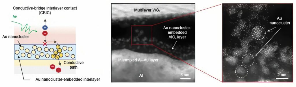
A 2D electrode material called a conductive-bridge interlayer contact enables an image sensor with high optical signal efficiency. This incorporates gold nanoparticles within the electrode, significantly reducing resistance and boosting performance. It also addresses the issue of Fermi-level pinning, which is a common challenge in conventional electrode materials that reduces a sensor’s optical signal efficiency. The developed electrode material is easy to fabricate and scalable for image sensors.
Acknowledgements
With thanks to José María Pulido at UAV Navigation-Grupo Oesía, Hervé Bouaziz at Lynred and Do Kyung Hwang of the Post-Silicon Semiconductor Institute at the Korea Institute of Science and Technology (KIST).
UPCOMING EVENTS


