


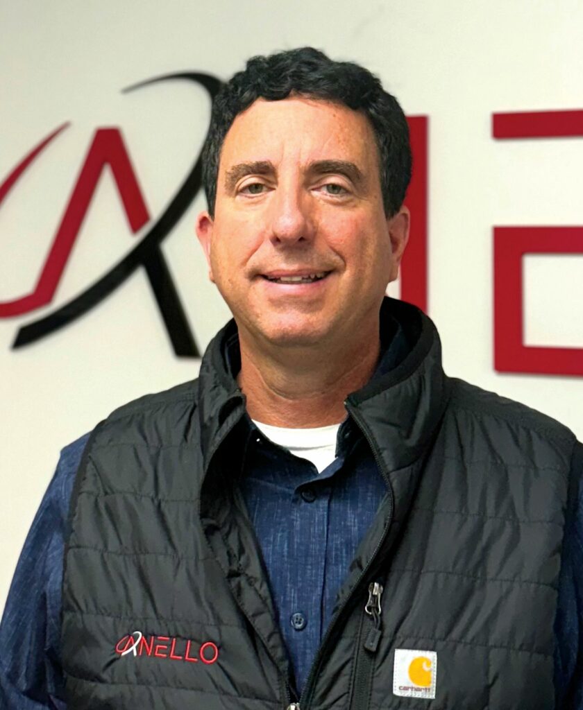
In conversation: Mario Paniccia

(Image: Spc Nicole Miller, US Army)
Optical revolutionary
Mario Paniccia, a guiding light in the field of high-speed data transmission using silicon photonics technology, talks to Peter Donaldson
At Intel, Mario Paniccia proved that silicon can transmit and receive data using light, thereby pioneering silicon photonics, which has applications in communications, AI, sensing, biomedical and beyond. He subsequently used this knowledge to invent silicon-chip-based optical inertial sensors with performance that enables GNSS-independent navigation systems sufficiently compact for small uncrewed vehicles and potentially for mass-market handheld devices.
Born in 1966 to working class Italian immigrants, Paniccia grew up in the town of Endicott in upstate New York, and showed technical curiosity and aptitude from childhood. His parents Antonio and Domenica Paniccia grew up working on family farms in Italy after World War II and had little formal education. They immigrated to the US in 1958. Young Mario took jobs from around age 12, earning money from landscaping, working in restaurants and helping his uncles on construction projects during weekends and summer holiday. However, his academic results earned him a place at Binghamton University to study physics.
There, he met Professor Robert Pompi, who inspired him to pursue an advanced degree and encouraged him to apply to top US academic institutions. That effort yielded a summer internship at Rutgers University, followed by a second at AT&T Bell Labs and, later, a third with IBM TJ Watson at Yorktown Heights. “Those experiences were invaluable in showing me how real science and research were done, and shaped my career.”
The internship at IBM brought him into contact with Atomic Force Microscopy, sparking an interest in this means of creating three-dimensional nanoscale images of surfaces and the complementary technique of Scanning Tunnelling Microscopy (STM). This inspired his PhD thesis, undertaken at Purdue University.
“When I went to Purdue, Professor Ron Reifenberger was starting work in this area, so I decided to join his group,” he recalls. “I had worked at Intel for a year and was learning about electromigration in integrated circuits, so I thought I would study how that effect happened at the atomic level. Therefore, I combined the two concepts and studied how atoms moved under the effects of high current densities using STM.”
Seeing the light
He joined Intel in 1995, where he developed a laser voltage probe used to measure real-time transistor switching in a fully running microprocessor by shining an infrared laser through the backside of the microprocessor chip. “That technology is still used today to debug running microprocessors in real time across the semiconductor industry.”
The concept of using infrared light to read transistor switching inspired him to ask himself whether light could be used to transmit data between chips. Key figures at Intel – including founder Gordon Moore, employee number four Les Vadasz and CTO Pat Gelsinger – liked the idea, leading to the foundation of the company’s Photonics Technology Lab.
A major breakthrough came with the demonstration of the world’s first gigahertz-speed silicon modulator – enabled in a silicon chip. “At that time, you have to remember that the fastest modulation in silicon was 10 MHz, and no one thought you could get anything faster than that.” Industry experts including Professor Graham Reed, then of Surrey University, validated that this was a sufficiently significant breakthrough that the team should submit their research results to the prestigious scientific journal Nature, Paniccia recalls. “It was when Nature accepted this for publication that everyone realised that we had done something very special.”
Silicon was not considered a good optical material at the time, however. “There were many, not just at Intel but around the world, who just said it was a waste of time,” he recalls. “But I kept telling the team: ‘Let’s prove everyone wrong.’ If we could do this, the value to the industry on being able to communicate optically with silicon would be game-changing. So, we went from demonstrating 1 GHz to 10 GHz to 40 GHz modulation in a span of a few years. We developed a hybrid silicon laser, where we heterogeneously bonded indium phosphide onto silicon to create integrated lasers on a silicon platform. We demonstrated a Raman silicon laser and photodetectors that were capable of running at 40 GHz. Before you knew it, we had all the building blocks that showed that this could really work.”
Proof came in July 2010 when the team demonstrated an integrated optical link that transmitted real data between two silicon photonic chips at 50 Gbps, at a time when the telecom industry standard was 10 Gbps and PCs were employing USB technology running at just 10 Mbps. This demonstration showed the potential for vast bandwidth increases with integrated silicon photonics.
Reflecting on his 21 years at Intel, Paniccia emphasises that he is most proud of the people he was able to attract and forge into a small team that did not know what was not possible. “We created an entirely new field,” he says. “Many of my team are now leading activities at all the major transceiver companies and GPU companies like NVIDIA, AMD, CISCO, Lumentum and others in Silicon Valley, or they have their own startups.”
Risk & reward
After Intel, Paniccia spent almost four years at Versalume – a light-emitting fibre startup spun out from Corning – gaining experience that helped when the time came to bring the Silicon Photonics Optical Gyro (SiPhOG) to the navigation market with ANELLO, which launched in 2020.
The biggest technical risk the new company faced stemmed from the lack of models for the design and fabrication of their specialised photonic chips. “We are building a very sensitive interferometer designed to measure 50 nanoradians of phase shift,” he explains. “So, we had to design, fabricate and test these devices using models that we developed from scratch, then tweak the models and re-design, fabricate and re-test. This took significant time and effort, but today we have the ability to predict very accurately how what we’re building will perform.”
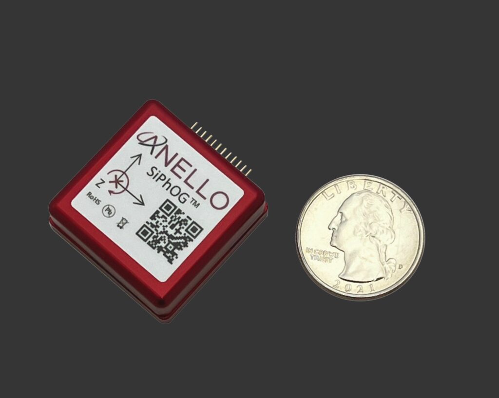
(Image: ANELLO Photonics)
While ANELLO had a tough start because of the COVID-19 pandemic, the timing was much better for SiPhOG’s debut because the Ukraine war brought awareness of the need to counter GPS jamming and spoofing to a peak.
Paniccia’s current priority is to ramp up production to meet demand. He emphasises that the key to mass production is to design for high volume from the beginning, not only at Photonic Integrated Chip (PIC) level but also at whole system level. This means addressing a range of assembly challenges, from attaching the tiny laser that injects light into the photonic circuits to precise positioning of the PIC on the printed circuit board, all in a manner that supports automated assembly with fast pick-and-place machines. This is possible, he explains, thanks to a team with extensive mass-production experience and partnerships with leading high-volume chip foundry Tower Semiconductor and manufacturing experts.
In the spotlight
Like the familiar Fibre-Optic Gyro, SiPhOG is a self-contained, low-drift-rate inertial sensor, the optical core of which is also insensitive to temperature, vibration and electromagnetic interference. SiPhOG is then put into a system with a CPU, GNSS chips and ANELLO’s algorithms to produce an inertial navigation system (INS) that, uniquely, can take over the navigation task when the algorithms detect that the satellite signal has been blocked, jammed or spoofed.
“The tricky part was spoofing. How do you know if the satellite signal is good or bad when the signal strength shows it is working? Thanks to the accuracy of SiPhOG and the INS, we realised that we can compare our position in real time with GPS every 10 ms, and if they diverge significantly, we can instantaneously flag that something is wrong.”
Developing new technology, Paniccia says, involves getting people and teams to do things that they thought were not possible. “You need to challenge them, guide them, give them direction and keep pushing them not to give up when things don’t work the first time,” he emphasises.
While he reckons that his leadership style is much the same as it was at Intel, he believes he has calmed with age. He confesses to being as excited as ever about new technology and still driven to prove doubters wrong.
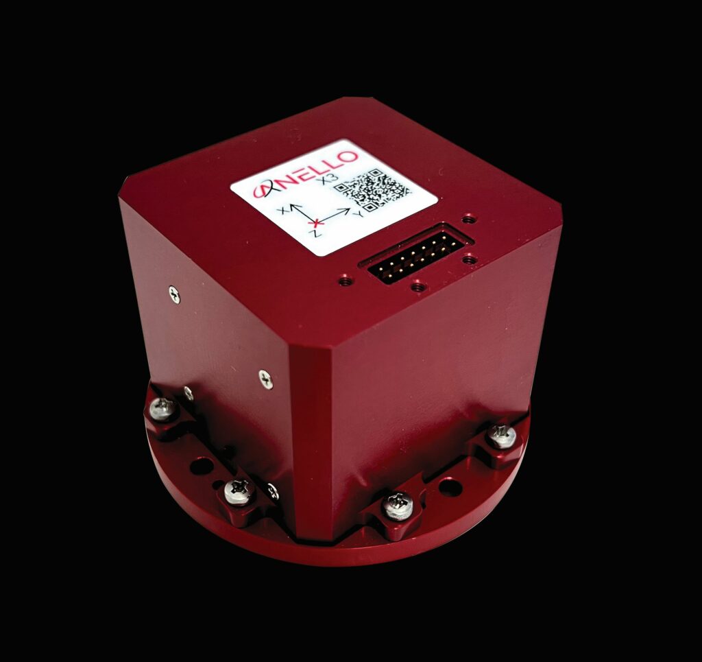
(Image: ANELLO Photonics)
Open forums with the team are more frequent than before, particularly when they need more guidance to achieve ‘bold’ goals and the natural fear of failure needs to be managed. When hiring, he values the ability to work in multidisciplinary teams as highly as technical skills.
Fostering a culture of innovation while maintaining focus on delivering for customers is hard, as R&D and testing new ideas are very different from volume production and shipping. “I often tell the innovation and research people to ‘walk through’ a product life cycle and see how to take an idea through to production,” he says.
ANELLO is now delivering SiPhOG-enabled navigation systems for land, sea and air applications, and Paniccia anticipates that further system-level integration will bring smaller form factors, lower power consumption and higher production volumes. This will enable the next step into handheld devices, robots, very small drones, smartphones and wearables.
Beacon of hope
While SiPhOG relies on the same Sagnac interferometry technique as other laser gyros, the next optical inertial sensor technology the company is developing relies on sustained optical resonance. This is generated in a silicon nitride ring with a quality factor of 100 million or more, meaning that the light loses very little energy as it circulates around the ring, thanks to a very-low-loss – and proprietary – silicon nitride process. This creates an enormous effective optical path length, which is the key to the sensor’s angular measurement sensitivity. The light propagates in a standing wave pattern with a specific frequency. As the ring rotates, the frequency shifts and measuring the shift reveals the angular rate of the platform, Paniccia explains.
“These rings can be quite small – of the order of five to 10 mm in diameter – so you can get a high-performance gyro on a very small footprint.” This opens up consumer and high-volume applications.
“The key challenge is not the ring resonators but engineering the whole system because you need a narrow line width laser, you need tuning and you need a different feedback system. All of these could be integrated on a single chip.”
Beyond ANELLO, Paniccia is working to bring high-volume silicon photonics to applications from data centres, ‘compute’ and AI to Lidar and more through an open silicon photonics foundry. The vehicle for this is the OpenLight company – of which Paniccia is chairman – which is behind Photonic Application Specific Integrated Circuit technology created to underpin custom devices. “OpenLight is about enabling customers to design their own highly integrated photonics chips based on heterogeneous integration and take them to the mass market.”
He often gives lectures on university campuses to students about innovation and risk-taking. “Don’t have regrets,” he tells them. “Don’t look back on life and lament not doing this or that. Don’t be afraid to fail. Take risks when you’re young, but don’t assume there is a simple or clear path ahead. Innovation and new business are hard and can take a long time, so you have to put in the time.”
Paniccia is most proud of his wife and of his two sons, and to the latter he gives the same advice as he does others, “I don’t care what you do in life; just find your passion and give it your all.”
Mario Paniccia
Mario Paniccia is a pioneer in silicon photonics, the enabling technology for high-speed connectivity used in data centres, for compute, AI systems, Lidar and for low-drift-rate microscale optical inertial sensors. He earned a bachelor’s degree in physics from Binghamton University in 1988 and went on to complete summer internships at AT&T Bell Labs in 1989 and IBM TJ Watson research in 1990. He undertook a PhD in physics at Purdue University, publishing his thesis, titled ‘Scanning Probe Studies of Electromigration in Gold Films’, in 1994.
This led to a 21 year career at Intel during which he founded and managed its Silicon Photonics Technology Lab, becoming an Intel Fellow in 2007, then general manager of the new Silicon Photonics Solutions Group formed to commercialise integrated silicon photonics in 2012, becoming CTO in January 2015. After Intel, he became an advisor and investor to startups in the San Francisco Bay Area. He joined startup Versalume in 2016 as founding CEO, starting ANELLO Photonics in 2020, where he serves as chairman and CEO. Paniccia has over 80 patents. He is a Fellow of the IEEE, SPIE and OSA. In February 2021, Paniccia was inducted into the National Academy of Engineers for his contributions to and commercialisation of silicon photonics.
UPCOMING EVENTS


